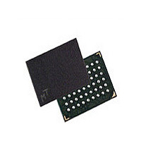
MT45W1MW16BDGB-708 WT Micron Technology Inc, MT45W1MW16BDGB-708 WT Datasheet - Page 26

MT45W1MW16BDGB-708 WT
Manufacturer Part Number
MT45W1MW16BDGB-708 WT
Description
Manufacturer
Micron Technology Inc
Datasheet
1.MT45W1MW16BDGB-708_WT.pdf
(59 pages)
Specifications of MT45W1MW16BDGB-708 WT
Operating Temperature (max)
85C
Mounting
Surface Mount
Operating Temperature Classification
Commercial
Lead Free Status / RoHS Status
Compliant
Figure 20:
Latency Counter (BCR[13:11]) Default = Three-Clock Latency
Operating Mode (BCR[15]) Default = Asynchronous Operation
Table 5:
Figure 21:
PDF: 09005aef81cb58ed/Source: 09005aef81c7a667
16mb_burst_cr1_0_p23z_2.fm - Rev. H 4/08 EN
Latency Configuration Code
2 (3 clocks)
3 (4 clocks) – default
DQ[15:0]
DQ[15:0]
DQ[15:0]
A[19:0]
WAIT
WAIT
ADV#
CLK
CLK
Latency Configuration
V
V
V
V
V
V
V
V
V
V
WAIT Configuration During Burst Operation
Latency Counter
IH
IL
IH
IL
IH
IL
OH
OL
OH
OL
Note:
ADDRESS
VALID
The latency counter bits determine how many clocks occur between the beginning of a
READ or WRITE operation and the first data value transferred. Only latency code two
(three clocks) or latency code three (four clocks) is allowed (see Table 5 and Figure 21).
The operating mode bit selects either synchronous BURST operation or the default
asynchronous mode of operation.
Non-default BCR setting for WAIT during BURST operation: WAIT active LOW.
Code 3
Code 2
16Mb: 1 Meg x 16 Async/Page/Burst CellularRAM 1.0 Memory
D[0]
(Default)
D[1]
26
OUTPUT
VALID
104 (9.62ns)
104 MHz
66 (15ns)
D[2]
Micron Technology, Inc., reserves the right to change products or specifications without notice.
Max Input CLK Frequency (MHz)
OUTPUT
OUTPUT
VALID
VALID
D[3]
OUTPUT
OUTPUT
VALID
VALID
DON’T CARE
Configuration Registers
DON’T CARE
D[4]
©2005 Micron Technology, Inc. All rights reserved.
OUTPUT
OUTPUT
VALID
VALID
53 (18.75ns)
80 (12.50ns)
BCR[8] = 0
Data valid in current cycle.
BCR[8] = 1
Data valid in next cycle.
80 MHz
UNDEFINED
OUTPUT
OUTPUT
VALID
VALID


