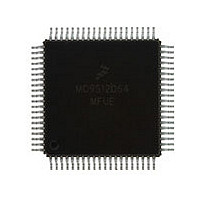
MC9S12D64MFUE Freescale, MC9S12D64MFUE Datasheet - Page 64

MC9S12D64MFUE
Manufacturer Part Number
MC9S12D64MFUE
Description
Manufacturer
Freescale
Datasheet
1.MC9S12D64MFUE.pdf
(128 pages)
Specifications of MC9S12D64MFUE
Cpu Family
HCS12
Device Core Size
16b
Frequency (max)
25MHz
Interface Type
CAN/I2C/SCI/SPI
Total Internal Ram Size
4KB
# I/os (max)
49
Number Of Timers - General Purpose
8
Operating Supply Voltage (typ)
2.5/5V
Operating Supply Voltage (max)
2.75/5.25V
Operating Supply Voltage (min)
2.35/4.5V
On-chip Adc
2(8-chx10-bit)
Instruction Set Architecture
CISC
Operating Temp Range
-40C to 125C
Operating Temperature Classification
Automotive
Mounting
Surface Mount
Pin Count
80
Package Type
PQFP
Program Memory Type
Flash
Program Memory Size
64KB
Lead Free Status / RoHS Status
Compliant
Available stocks
Company
Part Number
Manufacturer
Quantity
Price
Company:
Part Number:
MC9S12D64MFUE
Manufacturer:
Freescale Semiconductor
Quantity:
10 000
MC9S12DJ64 Device User Guide — V01.20
2.3.55 PS2 / RXD1 — Port S I/O Pin 2
PS2 is a general purpose input or output pin. It can be configured as the receive pin RXD of Serial
Communication Interface 1 (SCI1).
2.3.56 PS1 / TXD0 — Port S I/O Pin 1
PS1 is a general purpose input or output pin. It can be configured as the transmit pin TXD of Serial
Communication Interface 0 (SCI0).
2.3.57 PS0 / RXD0 — Port S I/O Pin 0
PS0 is a general purpose input or output pin. It can be configured as the receive pin RXD of Serial
Communication Interface 0 (SCI0).
2.3.58 PT[7:0] / IOC[7:0] — Port T I/O Pins [7:0]
PT7-PT0 are general purpose input or output pins. They can be configured as input capture or output
compare pins IOC7-IOC0 of the Enhanced Capture Timer (ECT).
2.4 Power Supply Pins
MC9S12DJ64 power and ground pins are described below.
64
NOTE:
Mnemonic
VDD1, 2
VSS1, 2
VDDR
VSSR
VDDX
VDDA
VSSX
VSSA
VRH
VRL
Table 2-2 MC9S12DJ64 Power and Ground Connection Summary
All VSS pins must be connected together in the application.
112-pin QFP
Pin Number
13, 65
14, 66
107
106
41
40
83
86
85
84
Nominal
Voltage
2.5V
5.0V
5.0V
5.0V
5.0V
0V
0V
0V
0V
0V
Internal power and ground generated by internal regulator
External power and ground, supply to pin drivers and internal
External power and ground, supply to pin drivers.
Operating voltage and ground for the analog-to-digital
Reference voltages for the analog-to-digital converter.
voltage regulator.
converters and the reference for the internal voltage regulator,
allows the supply voltage to the A/D to be bypassed
independently.
Description


