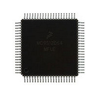
MC9S12D64MFUE Freescale, MC9S12D64MFUE Datasheet - Page 87

MC9S12D64MFUE
Manufacturer Part Number
MC9S12D64MFUE
Description
Manufacturer
Freescale
Datasheet
1.MC9S12D64MFUE.pdf
(128 pages)
Specifications of MC9S12D64MFUE
Cpu Family
HCS12
Device Core Size
16b
Frequency (max)
25MHz
Interface Type
CAN/I2C/SCI/SPI
Total Internal Ram Size
4KB
# I/os (max)
49
Number Of Timers - General Purpose
8
Operating Supply Voltage (typ)
2.5/5V
Operating Supply Voltage (max)
2.75/5.25V
Operating Supply Voltage (min)
2.35/4.5V
On-chip Adc
2(8-chx10-bit)
Instruction Set Architecture
CISC
Operating Temp Range
-40C to 125C
Operating Temperature Classification
Automotive
Mounting
Surface Mount
Pin Count
80
Package Type
PQFP
Program Memory Type
Flash
Program Memory Size
64KB
Lead Free Status / RoHS Status
Compliant
Available stocks
Company
Part Number
Manufacturer
Quantity
Price
Company:
Part Number:
MC9S12D64MFUE
Manufacturer:
Freescale Semiconductor
Quantity:
10 000
Appendix A Electrical Characteristics
A.1 General
This introduction is intended to give an overview on several common topics like power supply, current
injection etc.
A.1.1 Parameter Classification
The electrical parameters shown in this supplement are guaranteed by various methods. To give the
customer a better understanding the following classification is used and the parameters are tagged
accordingly in the tables where appropriate.
P:
C:
T:
D:
A.1.2 Power Supply
The MC9S12DJ64 and MC9S12D32 utilize several pins to supply power to the I/O ports, A/D converter,
oscillator, PLL and internal logic.
The VDDA, VSSA pair supplies the A/D converter and the resistor ladder of the internal voltage regulator.
The VDDX, VSSX, VDDR and VSSR pairs supply the I/O pins, VDDR supplies also the internal voltage
regulator.
VDD1, VSS1, VDD2 and VSS2 are the supply pins for the digital logic, VDDPLL, VSSPLL supply the
oscillator and the PLL.
VSS1 and VSS2 are internally connected by metal.
NOTE:
Those parameters are guaranteed during production testing on each individual device.
Those parameters are achieved by the design characterization by measuring a statistically relevant
sample size across process variations.
Those parameters are achieved by design characterization on a small sample size from typical devices
under typical conditions unless otherwise noted. All values shown in the typical column are within
this category.
Those parameters are derived mainly from simulations.
This classification is shown in the column labeled “C” in the parameter tables
where appropriate.
MC9S12DJ64 Device User Guide — V01.20
87


