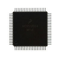
MC9S12D64MFUE Freescale, MC9S12D64MFUE Datasheet - Page 91

MC9S12D64MFUE
Manufacturer Part Number
MC9S12D64MFUE
Description
Manufacturer
Freescale
Datasheet
1.MC9S12D64MFUE.pdf
(128 pages)
Specifications of MC9S12D64MFUE
Cpu Family
HCS12
Device Core Size
16b
Frequency (max)
25MHz
Interface Type
CAN/I2C/SCI/SPI
Total Internal Ram Size
4KB
# I/os (max)
49
Number Of Timers - General Purpose
8
Operating Supply Voltage (typ)
2.5/5V
Operating Supply Voltage (max)
2.75/5.25V
Operating Supply Voltage (min)
2.35/4.5V
On-chip Adc
2(8-chx10-bit)
Instruction Set Architecture
CISC
Operating Temp Range
-40C to 125C
Operating Temperature Classification
Automotive
Mounting
Surface Mount
Pin Count
80
Package Type
PQFP
Program Memory Type
Flash
Program Memory Size
64KB
Lead Free Status / RoHS Status
Compliant
Available stocks
Company
Part Number
Manufacturer
Quantity
Price
Company:
Part Number:
MC9S12D64MFUE
Manufacturer:
Freescale Semiconductor
Quantity:
10 000
A.1.8 Power Dissipation and Thermal Characteristics
Power dissipation and thermal characteristics are closely related. The user must assure that the maximum
operating junction temperature is not exceeded. The average chip-junction temperature (T
obtained from:
T J
NOTE:
I/O, Regulator and Analog Supply Voltage
Digital Logic Supply Voltage
PLL Supply Voltage
Voltage Difference VDDX to VDDR and VDDA
Voltage Difference VSSX to VSSR and VSSA
Oscillator
Bus Frequency
MC9S12DJ64C
MC9S12DJ64V
MC9S12DJ64M
=
NOTES:
1. The device contains an internal voltage regulator to generate the logic and PLL supply out of the I/O supply. The
2. Some blocks e.g. ATD (conversion) and NVMs (program/erase) require higher bus frequencies for proper oper-
3. Please refer to Section A.1.8 Power Dissipation and Thermal Characteristics for more details about the rela-
Junction Temperature, [ C
given operating range applies when this regulator is disabled and the device is powered from an external source.
ation.
tion between ambient temperature T
Operating Ambient Temperature Range
Operating Ambient Temperature Range
Operating Ambient Temperature Range
Please refer to the temperature rating of the device (C, V, M) with regards to the
ambient temperature T
calculations refer to Section A.1.8 Power Dissipation and Thermal
Characteristics.
Operating Junction Temperature Range
Operating Junction Temperature Range
Operating Junction Temperature Range
1
Rating
1
Table A-4 Operating Conditions
A
A
and device junction temperature T
T J
and the junction temperature T
=
T A
3
3
3
+
Symbol
V
V
DDPLL
V
VDDX
VSSX
f
f
P D
T
T
T
DD5
osc
bus
T
T
T
DD
A
A
A
J
J
J
JA
MC9S12DJ64 Device User Guide — V01.20
0.25
Min
2.35
2.35
-0.1
-0.1
4.5
0.5
-40
-40
-40
-40
-40
-40
2
J
.
J
. For power dissipation
Typ
2.5
2.5
27
27
27
5
0
0
-
-
-
-
-
Max
5.25
2.75
2.75
100
120
105
140
125
0.1
0.1
16
25
85
J
) in C can be
Unit
MHz
MHz
V
V
V
V
V
C
C
C
C
C
C
91


