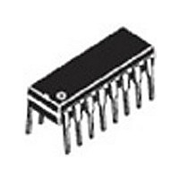
SN74LS221NG ON Semiconductor, SN74LS221NG Datasheet - Page 4

SN74LS221NG
Manufacturer Part Number
SN74LS221NG
Description
Manufacturer
ON Semiconductor
Datasheet
1.SN74LS221NG.pdf
(7 pages)
Specifications of SN74LS221NG
Logic Family
LS
High Level Output Current
-400uA
Low Level Output Current
8mA
Quiescent Current
11uA
Number Of Elements
2
Operating Temperature Classification
Commercial
Operating Supply Voltage (max)
5.25V
Operating Supply Voltage (typ)
5V
Operating Temperature (min)
0C
Operating Temperature (max)
70C
Technology
Bipolar
Abs. Propagation Delay Time
80ns
Operating Supply Voltage (min)
4.75V
Lead Free Status / RoHS Status
Compliant
DC CHARACTERISTICS OVER OPERATING TEMPERATURE RANGE
Note 1: Not more than one output should be shorted at a time, nor for more than 1 second.
V
V
V
V
V
V
V
V
V
I
I
I
I
IH
IL
OS
CC
T+
T−
T+
T−
IH
IL
IK
OH
OL
Symbol
Positive-Going Threshold
Voltage at C Input
Negative-Going Threshold
Voltage at C Input
Positive-Going Threshold
Voltage at B Input
Negative-Going Threshold
Voltage at B Input
Input HIGH Voltage
Input LOW Voltage
Input Clamp Voltage
Output HIGH Voltage
Output LOW Voltage
Input HIGH Current
Input LOW Current
Short Circuit Current (Note 1)
Power Supply Current
Input A
Input B
Clear
Quiescent
Triggered
Parameter
Min
−20
0.7
0.8
2.0
2.7
http://onsemi.com
Limits
0.35
Typ
1.0
0.8
1.0
0.9
3.4
4.7
19
4
−100
Max
−1.5
−0.4
−0.8
−0.8
2.0
2.0
0.8
0.5
0.1
20
11
27
(unless otherwise specified)
Unit
mA
mA
mA
mA
μA
V
V
V
V
V
V
V
V
V
V
V
V
V
Guaranteed Input HIGH Voltage for
A Input
Guaranteed Input LOW Voltage for
A Input
V
V
I
V
V
V
V
V
OL
CC
CC
CC
CC
CC
CC
CC
CC
CC
CC
CC
= 8.0 mA
= MIN
= MIN
= MIN
= MIN
= MIN, I
= MIN, I
= MAX, V
= MAX, V
= MAX, V
= MAX
= MAX
IN
OH
Test Conditions
IN
IN
IN
= − 18 mA
= MAX
= 2.7 V
= 7.0 V
= 0.4 V
V
CC
= MIN


