BTS621L1E3128AT Infineon Technologies, BTS621L1E3128AT Datasheet
BTS621L1E3128AT
Specifications of BTS621L1E3128AT


Related parts for BTS621L1E3128AT


BTS621L1E3128AT Summary of contents
Page 1
... Loss of ground and loss of V protection bb Electrostatic discharge (ESD) protection Application C compatible power switch with diagnostic feedback for 12 V and grounded loads All types of resistive, inductive and capacitve loads Replaces electromechanical relays, fuses and discrete circuits General Description N channel vertical power FET with charge pump, ground referenced CMOS compatible input and diagnostic feedback, monolithically integrated in Smart SIPMOS technology ...
Page 2
... Load current (Short circuit current, see page 5) Operating temperature range Storage temperature range Power dissipation (DC Inductive load switch-off energy dissipation, single pulse V = 12V 150°C, T j,start bb one channel, I both channels parallel, I see diagrams on page 9 Electrostatic discharge capability (ESD) (Human Body Model) acc ...
Page 3
... Thermal resistance chip - case, both channels: junction - ambient (free air): SMD version, device on PCB Electrical Characteristics Parameter and Conditions ° unless otherwise specified j bb Load Switching Capabilities and Characteristics On-state resistance (pin each channel Nominal load current, ISO Norm (pin 0 °C ON ...
Page 4
Parameter and Conditions ° unless otherwise specified j bb Operating Parameters ) Operating voltage 6 Undervoltage shutdown Undervoltage restart Undervoltage restart of charge pump see diagram page 13 Undervoltage hysteresis V = ...
Page 5
... V unless otherwise specified j bb Protection Functions 9) Initial peak short circuit current limit (pin Repetitive short circuit shutdown current limit (see timing diagrams, page 11 Output clamp (inductive load switch off mA OUT bb ON(CL) Thermal overload trip temperature Thermal hysteresis Reverse battery (pin ...
Page 6
... Delay time for status with open load after switch off (other channel in off state (see timing diagrams, page 12 Delay time for status with open load after switch off (other channel in on state (see timing diagrams, page 12 Status invalid after positive input slope ...
Page 7
Truth Table Normal operation Open load Short circuit Overtemperature Undervoltage/ Overvoltage L = "Low" Level X = don't care H = "High" Level Status signal after the time delay shown in the diagrams (see fig 5. page ...
Page 8
Status output R ST(ON) GND ESD-Zener diode: 6.1 V typ., max 5 mA; R < 380 at 1.6 mA, ESD zener diodes are not ST(ON used as voltage clamp at DC conditions. Operation in this mode may result ...
Page 9
... D are necessary. Semiconductor Group Inductive Load switch-off energy dissipation Energy stored in load inductance: While demagnetizing load inductance, the energy dissipated in PROFET with an approximate solution for Maximum allowable load inductance for a single switch off [mH] 10000 1000 100 PROFET ® BTS621L1 ...
Page 10
Typ. transient thermal impedance chip case Z = f(t ), one Channel active thJC p Z [K/W] thJC 10 1 0.1 0.01 1E-5 1E-4 1E-3 1E-2 Typ. transient thermal impedance chip case Z = f(t ), both Channel active thJC ...
Page 11
... OUT2 ST open drain Figure 2a: Switching a lamp OUT I L Semiconductor Group Both channels are symmetric and consequently the diagrams are valid for each channel as well as for permuted channels Figure 2b: Switching an inductive load OUT L(OL the time constant of load is too large, open-load-status may ...
Page 12
Figure 4a: Overtemperature: Reset if T < OUT T J Figure 5a: Open load: detection in ON-state, open load occurs in on-state IN1 IN2 channel 2: normal operation V OUT1 channel open ...
Page 13
Figure 6a: Undervoltage bb(under) V OUT ST open drain Figure 6b: Undervoltage restart of charge pump bb(over bb(o rst) bb(u rst) V bb(u cp) V bb(under) charge pump starts at V ...
Page 14
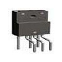
Package and Ordering Code All dimensions in mm Standard TO-220AB/7 BTS621L1 Q67060-S6304-A2 TO 220AB/7, Opt. E3230 BTS621L1 E3230 Q67060-S6304-A3 Semiconductor Group Ordering code SMD TO 220AB/7, Opt. E3128 BTS621L1 E3128A T&R: Changed since 04.96 Date Change Dec t d(ST OL4) ...
Page 15
... Due to technical requirements components may contain dangerous substances. For information on the types in question please contact your nearest Infineon Technologies Office. Infineon Technologies Components may only be used in life- support devices or systems with the express written approval of Infineon Technologies failure of such components can reasonably be expected to cause the failure of that life-support device or system affect the safety or effectiveness of that device or system ...