NUF6410MNT1G ON Semiconductor, NUF6410MNT1G Datasheet
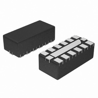
IC EMI FILTER 6LINE ESD 12-DFN

NUF6410MNT1G

Manufacturer Part Number
NUF6410MNT1G
Description
IC EMI FILTER 6LINE ESD 12-DFN
Manufacturer
ON Semiconductor
Datasheet

Specifications of NUF6410MNT1G

Resistance (ohms)
100
Capacitance
7pF
Power (watts)
0.6W
Package / Case
12-TDFN Exposed Pad
Resistance In Ohms
100
Product
EMI Filters
Maximum Dc Resistance
115 Ohms
Operating Temperature Range
- 40 C to + 85 C
Termination Style
SMD/SMT
Lead Free Status / RoHS Status
Lead free / RoHS Compliant
Tolerance
-
Lead Free Status / Rohs Status
Lead free / RoHS Compliant
Other names
NUF6410MNT1G
NUF6410MNT1GOSTR

Available stocks

Company
Part Number
Manufacturer
Quantity
Price
Part Number:
NUF6410MNT1G
Manufacturer:
ON Semiconductor
Quantity:
800
NUF6410MN
6-Channel EMI Filter with
Integrated ESD Protection
array with integrated ESD protection. Its typical component values of
R = 100 W and C = 7 pF deliver a cutoff frequency of 250 MHz and
stop band attenuation greater than −20 dB from 800 MHz to 3.0 GHz.
data rates up to 167 Mbps in applications where wireless interference
must be minimized. The specified attenuation range is very effective
in minimizing interference from 2G/3G, GPS, Bluetooth® and
WLAN signals.
x 3.0 mm DFN12 surface mount package.
Features/Benefits
Applications
© Semiconductor Components Industries, LLC, 2009
August, 2009 − Rev. 5
Filter + ESD
The NUF6410MN is a six−channel (C−R−C) Pi−style EMI filter
This performance makes the part ideal for parallel interfaces with
The NUF6010MU is available in the low−profile 12−lead 1.35 mm
Contact Discharge)
Characteristics of 250 MHz f
from 800 MHz to 3.0 GHz
Exceptional Cost, System Reliability and Space Savings
±8.0 kV ESD Protection on each channel (IEC61000−4−2 Level 4,
R/C Values of 100 W and 7 pF deliver Exceptional S21 Performance
Integrated EMI/ESD System Solution in DFN Package Offers
This is a Pb−Free Device
EMI Filtering for LCD and Camera Data Lines
EMI Filtering and Protection for I/O Ports and Keypads
n
Figure 1. Electrical Schematic
See Table 1 for pin description
C
d
= 7 pF
R = 100 W
3dB
C
d
= 7 pF
and −20 dB Stop Band Attenuation
Filter + ESD
n
1
−10
−15
−20
−25
−30
−35
−40
−45
−5
1.0E+6
0
Figure 2. Typical Insertion Loss Characteristic
†For information on tape and reel specifications,
NUF6410MNT1G
including part orientation and tape sizes, please
refer to our Tape and Reel Packaging Specifications
Brochure, BRD8011/D.
10.0E+6
Device
6410
M
G
(Note: Microdot may be in either location)
1
ORDERING INFORMATION
FREQUENCY (Hz)
http://onsemi.com
= Specific Device Code
= Date and Assembly Location
= Pb−Free Package
12
100.0E+6
(Pb−Free)
Package
CASE 506AD
DFN12
DFN12
Publication Order Number:
1.0E+9
3000 / Tape & Reel
Shipping
NUF6410MN/D
MARKING
DIAGRAM
1
MG
64
10
G
10.0E+9

Related parts for NUF6410MNT1G

NUF6410MNT1G Summary of contents

Page 1

... Semiconductor Components Industries, LLC, 2009 August, 2009 − Rev. 5 6410 M G (Note: Microdot may be in either location) Device NUF6410MNT1G †For information on tape and reel specifications, including part orientation and tape sizes, please refer to our Tape and Reel Packaging Specifications Brochure, BRD8011/D. 0 −5 − ...

Page 2

Table 1. FUNCTIONAL PIN DESCRIPTION Filter Filter 1 Filter 2 Filter 3 Filter 4 Filter 5 Filter 6 Ground Pad MAXIMUM RATINGS Parameter ESD Discharge IEC61000−4−2 DC Power per Resistor DC Power per Package Operating Temperature Range Storage Temperature Range ...

Page 3

TYPICAL PERFORMANCE CURVES 0 −5 −10 −15 −20 −25 −30 −35 −40 −45 1.0E+6 10.0E+6 100.0E+6 FREQUENCY (Hz) Figure 4. Typical Insertion Loss Characteristic 2 1 REVERSE VOLTAGE (V) Figure 6. Typical Capacitance ...

Page 4

... Therefore, to reasonably pass a square wave of frequency x the minimum filter bandwidth necessary is 3x. All ON Semiconductor EMI filters are rated according to this principle. Attempting to violate this principle will result in significant rounding of the waveform and cause problems in transmitting the correct data. For example, take the filter with the response shown in Figure 8 and apply three different data waveforms ...

Page 5

Table 2. Frequency Chart Bandwidth Maximum Supported Frequency 3 dB – 33.33 MHz ( 100 MHz 6 dB – 66.67 MHz ( 200 MHz 9 dB – 100 MHz ( 300 MHz Considering that ...

Page 6

... C 0.500 0.020 Pitch *For additional information on our Pb−Free strategy and soldering details, please download the ON Semiconductor Soldering and Mounting Techniques Reference Manual, SOLDERRM/D. N. American Technical Support: 800−282−9855 Toll Free USA/Canada Europe, Middle East and Africa Technical Support: Phone: 421 33 790 2910 Japan Customer Focus Center Phone: 81− ...

Related keywords