NUF4107FCT1G ON Semiconductor, NUF4107FCT1G Datasheet
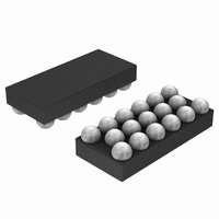
IC FILTER EMI ARRAY 4CH FLIPCHIP

NUF4107FCT1G

Manufacturer Part Number
NUF4107FCT1G
Description
IC FILTER EMI ARRAY 4CH FLIPCHIP
Manufacturer
ON Semiconductor
Datasheet

Specifications of NUF4107FCT1G

Resistance (ohms)
100
Capacitance
60pF
Power (watts)
0.6W
Package / Case
17-FlipChip
Resistance In Ohms
100
Lead Free Status / RoHS Status
Lead free / RoHS Compliant
Tolerance
-
Lead Free Status / Rohs Status
Compliant
Other names
NUF4107FCT1GOSTR

Available stocks

Company
Part Number
Manufacturer
Quantity
Price
Part Number:
NUF4107FCT1G
Manufacturer:
ON/安森美
Quantity:
20 000
NUF4107FC
Four Channel EMI Pi−Filter
Array with Full USB Filter
than −35 dB attenuation is obtained at frequencies from 800 MHz to
2.2 GHz. It also offers USB filtering circuitry with speed detection.
This includes the inline resistors for impedance matching and EMI
filtering. ESD protection is provided across all capacitors.
Features
Typical Applications
Stresses exceeding Maximum Ratings may damage the device. Maximum
Ratings are stress ratings only. Functional operation above the Recommended
Operating Conditions is not implied. Extended exposure to stresses above the
Recommended Operating Conditions may affect device reliability.
1. This does not include Pins B1, C1 and C2
*For additional information on our Pb−Free strategy and soldering details, please
© Semiconductor Components Industries, LLC, 2006
March, 2006 − Rev. 3
MAXIMUM RATINGS
download the ON Semiconductor Soldering and Mounting Techniques
Reference Manual, SOLDERRM/D.
ESD Discharge IEC61000−4−2 (Note 1)
Human Body Model
Machine Model
DC Power per Resistor
DC Power per Package
Junction Temperature
Operating Temperature Range
Storage Temperature Range
This device is a four−channel EMI filter array for data lines. Greater
EMI Filtering and ESD Protection for Data Lines
USB 1.1 Filtering Provided with Speed Detection
Integration of 27 Discretes Offers Cost and Space Savings
350 mm Solder Spheres
All TVS Protected Inputs Comply with IEC61000−4−2 (Level 4)
Low Profile Flip−Chip Packaging
MSL 1
All Pins Exceed 2000 V Human Body Model (Note 1)
Pb−Free Package is Available*
EMI and USB Filtering and ESD Protection for Data Lines
Cell Phones
Handheld Portables
Notebook Computers
MP3 Players
− Air Discharge, Contact Discharge
30 kV (Contact)
30 kV (Air)
Rating
(T
A
= 25°C)
Symbol
V
T
T
P
P
T
stg
PP
op
R
T
J
−55 to +150
−40 to +85
Value
100
600
150
0.4
30
16
1
Unit
mW
mW
kV
°C
°C
°C
†For information on tape and reel specifications,
NUF4107FCT1
NUF4107FCT1G
A1
A2
A3
A4
A5
A6
È
È
including part orientation and tape sizes, please
refer to our Tape and Reel Packaging Specifications
Brochure, BRD8011/D.
4107AYWW G
(Note: Microdot may be in either location)
Device
D
D
D
D
D
D
ORDERING INFORMATION
G
1
2
3
5
7
9
D
A1
CIRCUIT DESCRIPTION
11
MARKING DIAGRAM
http://onsemi.com
(Pb−Free)
Flip−Chip
Flip−Chip
Package
4107
A
Y
WW
G
B
B
B
B
C
C
C
C
C
C
2
3
4
5
7
9
5
1
2
3
Publication Order Number:
R
R
R
R
R
R
1
2
3
4
5
6
FLIP−CHIP−17
C
CASE 499AD
C
C
C
= Device Code
= Assembly Location
= Year
= Work Week
= Pb−Free Package
10
4
6
8
B
3000 Tape & Reel
3000 Tape & Reel
1
Shipping†
NUF4107FC/D
R
7
D
D
D
D
4
6
8
10
C1
C2
C3
C4
C5
C6

Related parts for NUF4107FCT1G

NUF4107FCT1G Summary of contents

Page 1

... ON Semiconductor Soldering and Mounting Techniques Reference Manual, SOLDERRM/D. © Semiconductor Components Industries, LLC, 2006 March, 2006 − Rev Symbol Value Unit 0.4 P 100 600 150 ° −40 to +85 ° −55 to +150 °C stg NUF4107FCT1 NUF4107FCT1G †For information on tape and reel specifications, 1 http://onsemi.com CIRCUIT DESCRIPTION ...

Page 2

ELECTRICAL CHARACTERISTICS Symbol 1 3.3 V per line − R EMI Filter Resistors USB Resistors; Impedance Matching USB Pull−up; Speed ...

Page 3

TEMPERATURE °C Figure 1. USB 1.1 Resistors (R1, R2) vs. Temperature 1600 1580 1560 1540 1520 1500 1480 1460 1440 1420 1400 −40 − TEMPERATURE °C ...

Page 4

Printed Circuit Board Recommendations Parameter PCB Pad Size Pad Shape Pad Type Solder Mask Opening Solder Stencil Thickness Stencil Aperture Solder Flux Ratio Solder Paste Type Trace Finish Trace Width Figure 7. Solder Mask versus Non−Solder Mask Definition − 280 ...

Page 5

... American Technical Support: 800−282−9855 Toll Free USA/Canada Japan: ON Semiconductor, Japan Customer Focus Center 2−9−1 Kamimeguro, Meguro−ku, Tokyo, Japan 153−0051 Phone: 81−3−5773−3850 http://onsemi.com 5 NOTES: 1. DIMENSIONING AND TOLERANCING PER ASME Y14.5M, 1994. 2. CONTROLLING DIMENSION: MILLIMETER. ...

Related keywords