TP3057WM National Semiconductor, TP3057WM Datasheet

TP3057WM

Manufacturer Part Number
TP3057WM
Description
Manufacturer
National Semiconductor
Type
PCMr
Datasheet

Specifications of TP3057WM

Number Of Channels
1
Gain Control
Adjustable
Number Of Adc's
1
Number Of Dac's
1
Package Type
SOIC W
Operating Supply Voltage (typ)
±5V
Number Of Adc Inputs
1
Number Of Dac Outputs
1
Operating Supply Voltage (max)
±5.25V
Operating Supply Voltage (min)
±4.75V
Operating Temperature (max)
85C
Operating Temperature (min)
-40C
Pin Count
16
Mounting
Surface Mount
Lead Free Status / RoHS Status
Not Compliant

Available stocks

Company
Part Number
Manufacturer
Quantity
Price
Part Number:
TP3057WM
Manufacturer:
NSC
Quantity:
370
Part Number:
TP3057WM
Manufacturer:
NS
Quantity:
2 503
Part Number:
TP3057WM
Manufacturer:
ST
0
Part Number:
TP3057WM
Manufacturer:
NS
Quantity:
20 000
Part Number:
TP3057WMX
Manufacturer:
NS/国半
Quantity:
20 000
C 1995 National Semiconductor Corporation
TP3054 TP3057
‘‘Enhanced’’ Serial Interface
CODEC Filter COMBO Family
General Description
The TP3054 TP3057 family consists of
monolithic PCM CODEC filters utilizing the A D and D A
conversion architecture shown in Figure 1 and a serial PCM
interface The devices are fabricated using National’s ad-
vanced double-poly CMOS process (microCMOS)
The encode portion of each device consists of an input gain
adjust amplifier an active RC pre-filter which eliminates very
high frequency noise prior to entering a switched-capacitor
band-pass filter that rejects signals below 200 Hz and above
3400 Hz Also included are auto-zero circuitry and a com-
panding coder which samples the filtered signal and en-
codes it in the companded -law or A-law PCM format The
decode portion of each device consists of an expanding
decoder which reconstructs the analog signal from the
companded
corrects for the sin x x response of the decoder output and
rejects signals above 3400 Hz followed by a single-ended
power amplifier capable of driving low impedance loads
The devices require two 1 536 MHz 1 544 MHz or 2 048
MHz transmit and receive master clocks which may be
asynchronous transmit and receive bit clocks which may
vary from 64 kHz to 2 048 MHz and transmit and receive
frame sync pulses The timing of the frame sync pulses and
PCM data is compatible with both industry standard formats
Connection Diagrams
COMBO and TRI-STATE are registered trademarks of National Semiconductor Corporation
Order Number TP3054WM or TP3057WM
Order Number TP3054N or TP3057N
Order Number TP3054J or TP3057J
See NS Package Number M16B
See NS Package Number N16A
See NS Package Number J16A
-law or A-law code a low-pass filter which
Dual-In-Line Package
Top View
TL H 5510
-law and A-law
TL H 5510– 1
Features
Y
Y
Y
Y
Y
Y
Y
Y
Y
Y
Y
Y
Complete CODEC and filtering system (COMBO)
including
A-law 16-pin TP3057
Designed for D3 D4 and CCITT applications
Low operating power typically 50 mW
Power-down standby mode typically 3 mW
Automatic power-down
TTL or CMOS compatible digital interfaces
Maximizes line interface card circuit density
Dual-In-Line or surface mount packages
See also AN-370 ‘‘Techniques for Designing with
CODEC Filter COMBO Circuits’’
g
-law 16-pin TP3054
5V operation
Transmit high-pass and low-pass filtering
Receive low-pass filter with sin x x correction
Active RC noise filters
Internal precision voltage reference
Serial I O interface
Internal auto-zero circuitry
-law or A-law compatible COder and DECoder
See NS Package Number V20A
Order Number TP3057V
Plastic Chip Carriers
Top View
RRD-B30M125 Printed in U S A
August 1994
TL H 5510– 10

Related parts for TP3057WM

TP3057WM Summary of contents

Page 1

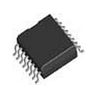
... Top View Order Number TP3054J or TP3057J See NS Package Number J16A Order Number TP3054N or TP3057N See NS Package Number N16A Order Number TP3054WM or TP3057WM See NS Package Number M16B COMBO and TRI-STATE are registered trademarks of National Semiconductor Corporation C 1995 National Semiconductor Corporation TL H 5510 ...

Page 2

Block Diagram Pin Description Symbol Function V Negative power supply pin GNDA Analog ground All signals are referenced to this pin VF O Analog output of the receive power ampli- R fier ...

Page 3

Functional Description POWER-UP When power is first applied power-on reset circuitry initializ- es the COMBO and places it into a power-down state All non-essential circuits are deactivated and the D outputs are put in high impedance states To power-up the ...

Page 4

Functional Description (Continued) TRANSMIT SECTION The transmit section input is an operational amplifier with provision for gain adjustment using two external resistors see Figure 4 The low noise and wide bandwidth allow gains in excess across the ...

Page 5

... Absolute Maximum Ratings If Military Aerospace specified devices are required please contact the National Semiconductor Sales Office Distributors for availability and specifications V to GNDA GNDA BB Voltage at any Analog Input or Output Electrical Characteristics are assured by correlation with other production tests and or product design and characterization All signals referenced to ...

Page 6

Timing Specifications Unless otherwise noted limits printed in BOLD characters are guaranteed for correlation with 100% electrical testing ...

Page 7

Timing Diagrams 7 ...

Page 8

Timing Diagrams (Continued) 8 ...

Page 9

Transmission Characteristics limits are assured by correlation with other production tests and or product design and characterization GNDA 1 02 kHz V 0 ...

Page 10

Transmission Characteristics guaranteed for All other limits are assured by correlation with other production tests and or product design and characterization GNDA kHz ...

Page 11

Transmission Characteristics guaranteed for All other limits are assured by correlation with other production tests and or product design and characterization GNDA kHz ...

Page 12

Applications Information POWER SUPPLIES While the pins of the TP305X family are well protected against electrical misuse it is recommended that the stan- dard CMOS practice be followed ensuring that ground is connected to the device before any other connections ...

Page 13

Applications Information (Continued) TABLE II Attentuator Tables for ...

Page 14

Connection Diagrams (Continued) Plastic Chip Carrier TL H 5510 – 7 Top View Order Number TP3057V See NS Package Number V20A 14 ...

Page 15

... Physical Dimensions inches (millimeters) Order Number TP3054WM or TP3057WM Cavity Dual-In-Line Package (J) Order Number TP3054J or TP3057J NS Package Number J16A Molded Small Outline Package (WM) NS Package Number M16B 15 ...

Page 16

... Hong Kong Ltd 49) 0-180-530 85 86 13th Floor Straight Block a Ocean Centre 5 Canton Rd 49) 0-180-530 85 85 Tsimshatsui Kowloon a Tel ( 49) 0-180-532 78 32 Hong Kong a 49) 0-180-532 93 58 Tel (852) 2737-1600 a Tel ( 49) 0-180-534 16 80 Fax (852) 2736-9960 a National Semiconductor Japan Ltd Tel 81-043-299-2309 Fax 81-043-299-2408 ...

Related keywords