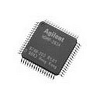
HDMP-2634 Avago Technologies US Inc., HDMP-2634 Datasheet - Page 2

HDMP-2634
Manufacturer Part Number
HDMP-2634
Description
Manufacturer
Avago Technologies US Inc.
Datasheet
1.HDMP-2634.pdf
(23 pages)
Specifications of HDMP-2634
Operating Supply Voltage (typ)
3.3V
Operating Temperature Classification
Commercial
Mounting
Surface Mount
Pin Count
64
Lead Free Status / RoHS Status
Not Compliant
Available stocks
Company
Part Number
Manufacturer
Quantity
Price
high-speed incoming clock and
data. The serial data is converted
back into 10-bit parallel data,
optionally recognizing the first
seven bits of the K28.5+ comma
character to establish byte align-
ment. If K28.5+ detection is en-
abled, the receiver section is able
to detect comma characters at
1.25 GBd or 2.5 GBd depending
on the value of the RX_RATE pin.
The recovered parallel data is
presented at SSTL_2 compatible
outputs RX[0:9], along with a
pair of 125 MHz SSTL_2 clocks,
RBC[0] and RBC[1], that are 180
degrees out of phase from one
another and which represent the
remote clock. Rising edges of
RBC[0] and RBC[1] may be used
to latch RX[0:9] data at the desti-
nation. Alternatively, both edges
of either RBC[1] or RBC[0] may
be used to latch Rx data (DDR).
The preceding applies when
RX_RATE=1 and RBC_SYNC=0.
For short distances, there may be
a need to have ASICs communi-
cate directly using parallel Tx and
Rx lines without the serdes inter-
mediary. To enable this, the Tx
and Rx parallel timing schemes
must be symmetrical. When
RBC_SYNC=1 and RX_RATE=1
such symmetry is obtained. In
this mode, the RX[0:9] lines
switch simultaneously with the
rising and falling edges of
RBC[1] or RBC[0] just as the
TX[0:9] lines switch simulta-
neously with TBC.
If RX_RATE=0 and RBC_SYNC=1
then the RX[0:9] lines switch
with the rising edges of RBC[1]
just as the TX[0:9] lines switch
with the rising edges of TBC. If
RBC_SYNC=0 then RX[0:9] data
may be latched on the rising
edges of RBC[1] and RBC[0]. In
this latter mode, the RBC[0:1]
clocks operate at a 62.5 MHz rate.
2
In summary, by setting
RBC_SYNC=0 the timing of
transmit and receive parallel data
with respect to TBC and
RBC[0:1] may be arranged so
that the upstream protocol device
can generate and latch data very
simply. This is the source cen-
tered mode of operation (case A
and C in Table 1, page 8). Alter-
natively, setting RBC_SYNC=1
provides for timing symmetry
between Tx and Rx parallel lines
at both 1.25 GBd and 2.5 GBd
rates. This is the source synchro-
nous mode of opertion (case B
and D in Table 1, page 8).
Note when EN_CDET=1, the first
transition of byte 0 of a comma
will either coincide with the rising
edge of RBC[1] or precede it.
This applies regardless of the
RX_RATE setting.
Table 1 summarizes the behavior
of the Rx parallel section under
all values of RX_RATE and
RBC_SYNC. For test purposes,
the transceiver provides for
on-chip parallel to parallel local
loopback functionality controlled
through the EWRAP pin. Addi-
tionally, the byte alignment fea-
ture via detection of the first
seven bits of the K28.5+ charac-
ter may be disabled. This may be
useful in proprietary applications
which use alternative methods to
align the parallel data.
The HDMP-2634 accepts either a
differential PECL or a LVTTL
reference clock input at 125 MHz.
HDMP-2634 Block Diagram
The HDMP-2634 (Figure 2) is
designed to transmit and receive
10-bit wide parallel data over
high-speed serial communication
lines. The parallel data applied to
the transmitter is expected to be
encoded per the 8B/10B encod-
ing scheme with special reserved
characters for link management
purposes. Other encoding
schemes will also work as long as
they provide DC balance and a
sufficient number of transitions.
The HDMP-2634 incorporates the
following:
• SSTL_2 Parallel I/O
• High Speed Phase Locked
• Parallel to Serial Converter
• High Speed Serial Clock and
• Comma Character Recognition
• Byte Alignment Circuitry
• Serial to Parallel Converter
INPUT LATCH
The transmitter accepts 10-bit
wide single ended SSTL_2
parallel data at inputs TX[0:9].
The SSTL_2 TBC clock provided
by the sender of the transmit data
is used as the transmit byte clock.
The TX[0:9] and TBC signals
must be properly aligned as
shown in Figure 3. If
TX_RATE=1, TX[0:9] data are
latched between both edges of
TBC. If TX_RATE=0, TX[0:9]
data are latched on the falling
edge of TBC. The TX[0:9] and
TBC inputs are unterminated
SSTL_2 inputs per section 4.1 of
the SSTL_2 standard (Figure 11).
TX PLL/CLOCK GENERATOR
The Transmitter Phase Locked
Loop and Clock Generator block
is responsible for generating all
internal clocks needed by the
transmitter section to perform its
functions. These clocks are based
on the supplied transmit byte
clock (TBC). Incoming data must
be synchronous with TBC
(Figures 3a-3b). Use of TBC to
determine sampling points to
latch data obviates the need for
PLLs in the data source.
Loops
Data Recovery Circuitry
per Fibre Channel
Specifications


