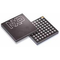
LPC1788FET208,551 NXP Semiconductors, LPC1788FET208,551 Datasheet - Page 40

LPC1788FET208,551
Manufacturer Part Number
LPC1788FET208,551
Description
MCU ARM 512K FLASH 208-TFBGA
Manufacturer
NXP Semiconductors
Series
LPC17xxr
Specifications of LPC1788FET208,551
Core Processor
ARM® Cortex-M3™
Core Size
32-Bit
Speed
100MHz
Connectivity
CAN, EBI/EMI, Ethernet, I²C, Microwire, MMC, SPI, SSI, SSP, UART/USART, USB OTG
Peripherals
Brown-out Detect/Reset, DMA, I²S, LCD, Motor Control PWM, POR, PWM, WDT
Number Of I /o
165
Program Memory Size
512KB (512K x 8)
Program Memory Type
FLASH
Eeprom Size
4K x 8
Ram Size
96K x 8
Voltage - Supply (vcc/vdd)
2.4 V ~ 3.6 V
Data Converters
A/D 8x12b, D/A 1x10b
Oscillator Type
Internal
Operating Temperature
-40°C ~ 85°C
Package / Case
208-TFBGA
Processor Series
LPC178x
Core
ARM Cortex M3
Data Bus Width
32 bit
Data Ram Size
96 KB
Interface Type
SSP, I2S, USB, JTAG, Serial, UART, I2C, SD/MMC
Maximum Clock Frequency
100 MHz
Number Of Programmable I/os
165
Number Of Timers
4
Operating Supply Voltage
2.4 V to 3.6 V
Maximum Operating Temperature
+ 85 C
Mounting Style
SMD/SMT
Operating Temperature Range
- 40 C to + 85 C
Supply Current (max)
100 mA
Lead Free Status / Rohs Status
Lead free / RoHS Compliant
Other names
568-6691
Available stocks
Company
Part Number
Manufacturer
Quantity
Price
Company:
Part Number:
LPC1788FET208,551
Manufacturer:
NXP Semiconductors
Quantity:
10 000
NXP Semiconductors
Table 5.
Not all functions are available on all parts. See
7. Functional description
LPC178X_7X
Objective data sheet
Ball
Row J
1
5
9
13
Row K
1
5
9
13
Row L
1
5
9
13
Row M
1
5
9
13
Row N
1
5
9
13
Row P
1
5
9
13
Symbol
RESET
P0[13]
-
P0[18]
VBAT
P0[29]
P4[3]
P4[26]
P2[29]
P1[18]
V
V
P0[28]
P0[14]
P1[27]
P2[10]
P0[31]
P2[19]
V
P4[17]/EMC_A[17]
P2[24]
P1[19]
P2[16]
P4[4]
SS
SS
DD(REG)(3V3)
Pin allocation table TFBGA180
7.1 Architectural overview
The ARM Cortex-M3 includes three AHB-Lite buses: the system bus, the I-code bus, and
the D-code bus. The I-code and D-code core buses are faster than the system bus and
are used similarly to Tightly Coupled Memory (TCM) interfaces: one bus dedicated for
instruction fetch (I-code) and one bus for data access (D-code). The use of two core
buses allows for simultaneous operations if concurrent operations target different devices.
Ball Symbol
2
6
10
14
2
6
10
14
2
6
10
14
2
6
10
14
2
6
10
14
2
6
10
14
RTCX1
-
P0[19]
V
P1[31]
P1[20]
P4[6]
P0[20]
XTAL1
P4[0]
P0[10]
P0[22]
P2[28]
P1[22]
P0[0]
P4[19]
USB_D-2
P1[21]
P1[29]
P2[12]
P2[25]
P2[20]
P1[28]
P4[18]
DD(3V3)
All information provided in this document is subject to legal disclaimers.
Table 2
Rev. 2 — 27 May 2011
and
Table 7
Ball
3
7
11
3
7
11
3
7
11
3
7
11
3
7
11
3
7
11
(EMC pins).
Symbol
RTCX2
-
P4[8]
-
P1[30]
P3[26]
P0[21]
-
P0[27]
P1[25]
V
-
P3[25]
P4[1]
P2[13]
-
P3[24]
P1[23]
P0[1]
-
P2[18]
P1[24]
P2[17]
-
DD(3V3)
32-bit ARM Cortex-M3 microcontroller
Ball
4
8
12
4
8
12
4
8
12
4
8
12
4
8
12
4
8
12
LPC178x/7x
Symbol
P0[12]
-
P0[17]
-
XTAL2
V
P4[7]
-
V
V
P5[2]
-
P3[23]
P4[2]
P2[11]
-
P0[30]
P2[21]
P4[16]
-
V
P1[26]
P0[11]
-
DD(3V3)
DD(3V3)
SSREG
SS
© NXP B.V. 2011. All rights reserved.
40 of 117


