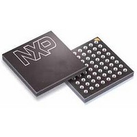
LPC1788FET208,551 NXP Semiconductors, LPC1788FET208,551 Datasheet - Page 52

LPC1788FET208,551
Manufacturer Part Number
LPC1788FET208,551
Description
MCU ARM 512K FLASH 208-TFBGA
Manufacturer
NXP Semiconductors
Series
LPC17xxr
Specifications of LPC1788FET208,551
Core Processor
ARM® Cortex-M3™
Core Size
32-Bit
Speed
100MHz
Connectivity
CAN, EBI/EMI, Ethernet, I²C, Microwire, MMC, SPI, SSI, SSP, UART/USART, USB OTG
Peripherals
Brown-out Detect/Reset, DMA, I²S, LCD, Motor Control PWM, POR, PWM, WDT
Number Of I /o
165
Program Memory Size
512KB (512K x 8)
Program Memory Type
FLASH
Eeprom Size
4K x 8
Ram Size
96K x 8
Voltage - Supply (vcc/vdd)
2.4 V ~ 3.6 V
Data Converters
A/D 8x12b, D/A 1x10b
Oscillator Type
Internal
Operating Temperature
-40°C ~ 85°C
Package / Case
208-TFBGA
Processor Series
LPC178x
Core
ARM Cortex M3
Data Bus Width
32 bit
Data Ram Size
96 KB
Interface Type
SSP, I2S, USB, JTAG, Serial, UART, I2C, SD/MMC
Maximum Clock Frequency
100 MHz
Number Of Programmable I/os
165
Number Of Timers
4
Operating Supply Voltage
2.4 V to 3.6 V
Maximum Operating Temperature
+ 85 C
Mounting Style
SMD/SMT
Operating Temperature Range
- 40 C to + 85 C
Supply Current (max)
100 mA
Lead Free Status / Rohs Status
Lead free / RoHS Compliant
Other names
568-6691
Available stocks
Company
Part Number
Manufacturer
Quantity
Price
Company:
Part Number:
LPC1788FET208,551
Manufacturer:
NXP Semiconductors
Quantity:
10 000
NXP Semiconductors
LPC178X_7X
Objective data sheet
7.17.1 Features
7.18.1 Features
7.18 12-bit ADC
7.19 10-bit DAC
Additionally, any pin on Port 0 and Port 2 providing a digital function can be programmed
to generate an interrupt on a rising edge, a falling edge, or both. The edge detection is
asynchronous, so it may operate when clocks are not present such as during Power-down
mode. Each enabled interrupt can be used to wake up the chip from Power-down mode.
The LPC178x/7x contain one ADC. It is a single 12-bit successive approximation ADC
with eight channels and DMA support.
The LPC178x/7x contain one DAC. The DAC allows to generate a variable analog output.
The maximum output value of the DAC is VREFP.
•
•
•
•
•
•
•
•
•
•
•
•
•
•
•
•
•
•
•
•
GPIO registers are accessed through the AHB multilayer bus so that the fastest
possible I/O timing can be achieved.
Mask registers allow treating sets of port bits as a group, leaving other bits
unchanged.
All GPIO registers are byte and half-word addressable.
Entire port value can be written in one instruction.
Support for Cortex-M3 bit banding.
Support for use with the GPDMA controller.
Bit level set and clear registers allow a single instruction to set or clear any number of
bits in one port.
Direction control of individual bits.
All I/O default to inputs after reset.
Pull-up/pull-down resistor configuration and open-drain configuration can be
programmed through the pin connect block for each GPIO pin.
12-bit successive approximation ADC.
Input multiplexing among eight pins.
Power-down mode.
Measurement range V
12-bit conversion rate: up to 400 kHz.
Individual channels can be selected for conversion.
Burst conversion mode for single or multiple inputs.
Optional conversion on transition of input pin or Timer Match signal.
Individual result registers for each ADC channel to reduce interrupt overhead.
DMA support.
All information provided in this document is subject to legal disclaimers.
Rev. 2 — 27 May 2011
SS
to VREFP.
32-bit ARM Cortex-M3 microcontroller
LPC178x/7x
© NXP B.V. 2011. All rights reserved.
52 of 117


