IDTCSPT855PGG IDT, Integrated Device Technology Inc, IDTCSPT855PGG Datasheet
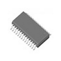
IC PLL CLK DRIVER 2.5V 28-TSSOP

IDTCSPT855PGG

Manufacturer Part Number
IDTCSPT855PGG
Description
IC PLL CLK DRIVER 2.5V 28-TSSOP
Manufacturer
IDT, Integrated Device Technology Inc
Type
PLL Clock Driverr
Series
-r
Datasheet

Specifications of IDTCSPT855PGG

Input
Clock
Output
Clock
Frequency - Max
220MHz
Voltage - Supply
2.3 V ~ 2.7 V
Operating Temperature
0°C ~ 70°C
Mounting Type
Surface Mount
Package / Case
28-TSSOP
Frequency-max
220MHz
Number Of Elements
1
Operating Supply Voltage (typ)
2.5V
Operating Temp Range
0C to 70C
Package Type
TSSOP
Operating Supply Voltage (min)
2.3V
Operating Supply Voltage (max)
2.7V
Operating Temperature Classification
Commercial
Pin Count
28
Lead Free Status / RoHS Status
Lead free / RoHS Compliant
Other names
CSPT855PGG

Available stocks

Company
Part Number
Manufacturer
Quantity
Price
Part Number:
IDTCSPT855PGG
Manufacturer:
IDT
Quantity:
629
Part Number:
IDTCSPT855PGGI
Manufacturer:
IDT
Quantity:
8 000
Part Number:
IDTCSPT855PGGI
Manufacturer:
IDT
Quantity:
20 000
FEATURES:
• PLL clock driver for DDR (Double Data Rate) synchronous
• Spread spectrum clock compatible
• Operating frequency: 60MHz to 220MHz
• Low jitter (cycle-to-cycle): ±50ps
• Distributes one differential clock input to four differential clock
• Enters low power mode and 3-state outputs when input CLK
• Operates from a 2.5V supply
• Consumes <200μ μ μ μ μ A quiescent current
• External feedback pins (FBIN, FBIN) are used to synchronize
• Available in TSSOP package
APPLICATIONS:
• For all DDR1 speeds: PC1600 (DDR200), PC2100 (DDR266),
The IDT logo is a registered trademark of Integrated Device Technology, Inc.
COMMERCIAL AND INDUSTRIAL TEMPERATURE RANGES
FUNCTIONAL BLOCK DIAGRAM
IDTCSPT855
2.5V PLL CLOCK DRIVER
c
DRAM applications
outputs
signal is less than 20MHz or PWRDWN is low
outputs to input clocks
PC2700 (DDR333), PC3200 (DDR400)
2008 Integrated Device Technology, Inc.
PWRDWN
FBIN
FBIN
CLK
CLK
AV
DD
6
7
23
22
24
9
2.5V PHASE LOCKED LOOP
CLOCK DRIVER
POWERDOWN
AND TEST
LOGIC
PLL
1
DESCRIPTION:
that distributes one differential clock input pair(CLK, CLK ) to four differential
output pairs (Y
(FBOUT, FBOUT). When PWRDWN is high, the outputs switch in phase and
frequency with CLK. When PWRDWN is low, all outputs are disabled to a high-
impedance state (3-state), and the PLL is shut down (low-power mode). The
device also enters this low-power mode when the input frequency falls below
a suggested detection frequency that is below 20MHz (typical 10MHz). An input
frequency detection circuit detects the low-frequency condition, and after
applying a >20MHz input signal, this detection circuit reactivates the PLL and
enables the outputs.
purposes. The CSPT855 is also able to track spread spectrum clocking for
reduced EMI.
to achieve phase-lock of the PLL. This stabilization time is required following
power up.
The CSPT855 is a high-performance, low-skew, low-jitter zero delay buffer
When AV
Since the CSPT855 is based on PLL circuitry, it requires a stabilization time
COMMERCIAL AND INDUSTRIAL TEMPERATURE RANGES
DD
[0:3]
is tied to GND, the PLL is turned off and bypassed for test
, Y
[0:3]
) and one differential pair of feedback clock outputs
12
13
17
16
26
27
19
20
3
2
Y0
Y0
Y1
Y1
Y2
Y2
Y3
Y3
FBOUT
FBOUT
NOVEMBER 2008
IDTCSPT855
DSC-6203/12

Related parts for IDTCSPT855PGG

IDTCSPT855PGG Summary of contents

Page 1

IDTCSPT855 2.5V PLL CLOCK DRIVER FEATURES: • PLL clock driver for DDR (Double Data Rate) synchronous DRAM applications • Spread spectrum clock compatible • Operating frequency: 60MHz to 220MHz • Low jitter (cycle-to-cycle): ±50ps • Distributes one differential clock input ...

Page 2

IDTCSPT855 2.5V PLL CLOCK DRIVER PIN CONFIGURATION 1 GND DDQ 5 GND CLK 6 7 CLK 8 V DDQ AGND V 11 DDQ ...

Page 3

IDTCSPT855 2.5V PLL CLOCK DRIVER FUNCTION TABLE (1) INPUTS PWRDWN AV CLK DD GND H L GND 2.5V (nom 2.5V (nom 2.5V (nom) X <20MHz NOTES ...

Page 4

IDTCSPT855 2.5V PLL CLOCK DRIVER DC ELECTRICAL CHARACTERISTICS OVER OPERATING RANGE Following Conditions Apply Unless Otherwise Specified: Commercial 0°C to +70°C; Industrial Symbol Parameter V Input Voltage (All Inputs HIGH-Level Output Voltage OH V ...

Page 5

IDTCSPT855 2.5V PLL CLOCK DRIVER SWITCHING CHARACTERISTICS Symbol Description PLH (2) t LOW to HIGH Level Propagation Delay Time PHL (2) t HIGH to LOW Level Propagation Delay Time JIT(PER) (3) t Jitter (period), see figure 6 JIT(CC) (3) t ...

Page 6

IDTCSPT855 2.5V PLL CLOCK DRIVER TEST CIRCUIT AND SWITCHING WAVEFORMS 60Ω 60Ω CSPT855 NOTE GND TT Yx, FBOUT Yx, FBOUT COMMERCIAL AND INDUSTRIAL TEMPERATURE RANGES R ...

Page 7

IDTCSPT855 2.5V PLL CLOCK DRIVER TEST CIRCUIT AND SWITCHING WAVEFORMS CLK CLK FBIN FBIN CLK CLK FBIN FBIN t D(Ø Yx, FBOUT Yx, FBOUT COMMERCIAL AND INDUSTRIAL TEMPERATURE RANGES t (Ø)n ∑ (Ø)n ...

Page 8

IDTCSPT855 2.5V PLL CLOCK DRIVER TEST CIRCUIT AND SWITCHING WAVEFORMS Yx, FBOUT Yx, FBOUT Yx, FBOUT Yx, FBOUT Yx, FBOUT Yx, FBOUT Yx, FBOUT Yx, FBOUT COMMERCIAL AND INDUSTRIAL TEMPERATURE RANGES t cycle ...

Page 9

IDTCSPT855 2.5V PLL CLOCK DRIVER TEST CIRCUIT AND SWITCHING WAVEFORMS 80% C lock Inputs and O utputs 20% COMMERCIAL AND INDUSTRIAL TEMPERATURE RANGES (I Figure 8. Input and Output Slew ...

Page 10

IDTCSPT855 2.5V PLL CLOCK DRIVER ORDERING INFORMATION XXXXX XX CSPT Package Device Type CORPORATE HEADQUARTERS 6024 Silver Creek Valley Road San Jose, CA 95138 COMMERCIAL AND INDUSTRIAL TEMPERATURE RANGES X Process Blank I PG PGG 855 for SALES: 800-345-7015 or ...

Related keywords