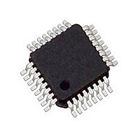
MC100EP196FAR2G ON Semiconductor, MC100EP196FAR2G Datasheet - Page 11

MC100EP196FAR2G
Manufacturer Part Number
MC100EP196FAR2G
Description
IC PROGRAM DELAY 3.3V ECL 32LQFP
Manufacturer
ON Semiconductor
Series
100EPr
Type
Programmable Delay Chipr
Datasheet
1.MC100EP196FAG.pdf
(18 pages)
Specifications of MC100EP196FAR2G
Input
ECL, LVCMOS, LVTTL
Output
ECL
Frequency - Max
1.2GHz
Voltage - Supply
3 V ~ 3.6 V
Operating Temperature
-40°C ~ 85°C
Mounting Type
Surface Mount
Package / Case
32-LQFP
Frequency-max
1.2GHz
Lead Free Status / RoHS Status
Lead free / RoHS Compliant
Other names
MC100EP196FAR2GOS
Available stocks
Company
Part Number
Manufacturer
Quantity
Price
Company:
Part Number:
MC100EP196FAR2G
Manufacturer:
SANYO
Quantity:
8 000
Company:
Part Number:
MC100EP196FAR2G
Manufacturer:
ON Semiconductor
Quantity:
10 000
NOTE: Device will meet the specifications after thermal equilibrium has been established when mounted in a test socket or printed circuit
8. Measured using a 750 mV source, 50% duty cycle clock source. All loading with 50 W to V
9. Specification limits represent the amount of delay added with the assertion of each individual delay control pin. The various combinations
10. The monotonicity indicates the increased delay value for each binary count increment on the control inputs D(0−9).
11. Duty cycle skew guaranteed only for differential operation measured from the cross point of the input to the cross point of the output.
12. This setup time defines the amount of time prior to the input signal the delay tap of the device must be set.
13. This setup time is the minimum time that EN must be asserted prior to the next transition of IN/IN to prevent an output response greater than
14. This hold time is the minimum time that EN must remain asserted after a negative going IN or positive going IN to prevent an output response
15. This release time is the minimum time that EN must be deasserted prior to the next IN/IN transition to ensure an output response that meets
Table 11. AC CHARACTERISTICS
f
t
t
t
Dt
Mono
t
t
t
t
t
V
t
t
Symbol
max
PLH
PHL
RANGE
SKEW
s
h
R
jit
r
f
PP
of asserted delay control inputs will typically realize D0 resolution steps across the specified programmable range.
V
greater than V
the specified IN to Q propagation delay and transition times.
CC
board with maintained transverse airflow greater than 500 lfpm. Electrical parameters are guaranteed only over the declared
operating temperature range. Functional operation of the device exceeding these conditions is not implied. Device specification limit
values are applied individually under normal operating conditions and not valid simultaneously.
− 1425 mV to that IN/IN transition.
Maximum Frequency
Propagation Delay
Programmable Range
Step Delay (Note 9)
Monotonicity (Note 10)
Duty Cycle Skew (Note 11)
Setup Time
Hold Time
Release Time
Random Clock Jitter
@ 1.2 GHz, SETMAX Delay
Input Voltage Swing
(Differential Configuration)
Output Rise/Fall Time
CC
− 1425 mV to that IN/IN transition.
{D(0−9) = HI} − {D(0−9) = LO}
Characteristic
IN to Q; D(0−9) = 1023
20−80% (CASCADE)
EN to Q; D(0−9) = 0
IN to Q; D(0−9) = 0
EN to IN (Note 13)
IN to EN (Note 14)
EN to IN (Note 15)
D10 to CASCADE
SET MAX to LEN
D to IN (Note 12)
SET MIN to LEN
20−80% (Q)
|t
PHL
V
D to LEN
LEN to D
D0 High
D1 High
D2 High
D3 High
D4 High
D5 High
D6 High
D7 High
D8 High
D9 High
CC
−t
= 0 V; V
PLH
|
1810
9500
1780
8600
1060
2160
4335
EE
Min
350
245
530
150
100
150
225
450
150
400
300
150
100
90
85
= −3.0 V to −3.6 V or V
http://onsemi.com
−40°C
11496
2210
2277
9285
2317
4647
−130
−105
−105
1158
Typ
450
137
293
590
−10
170
275
165
800
110
150
1.2
23
39
58
20
70
7
3
11
13500
10000
2610
2780
1265
2490
5010
1200
Max
550
185
335
650
130
200
10000
1960
1930
9200
2290
4590
1130
Min
380
100
260
560
150
100
150
200
450
150
400
350
150
110
95
CC
= 3.0 V to 3.6 V; V
12258
2360
2430
9897
1237
2472
4955
−150
−120
−120
25°C
Typ
477
149
313
629
−70
305
180
800
120
160
110
1.2
30
48
67
22
70
11
3
CC
14000
10700
− 2.0 V.
2760
2930
1355
2680
5385
1200
Max
580
200
370
710
145
210
EE
10955
2180
2150
9900
1200
2450
4935
Min
420
270
600
150
100
150
200
450
150
400
350
150
125
= 0 V (Note 8)
110
90
13454
10875
85°C
2580
2650
1353
2712
5440
−165
−140
−140
Typ
520
154
337
681
−70
325
160
205
800
135
175
1.2
13
32
53
73
27
60
3
15955
12000
2980
3150
1520
3015
6015
1200
Max
620
225
410
770
160
225
Unit
GHz
mV
ps
ps
ps
ps
ps
ps
ps
ps
ps
ps


