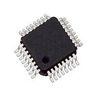
MC100EP196FAR2G ON Semiconductor, MC100EP196FAR2G Datasheet - Page 12

MC100EP196FAR2G
Manufacturer Part Number
MC100EP196FAR2G
Description
IC PROGRAM DELAY 3.3V ECL 32LQFP
Manufacturer
ON Semiconductor
Series
100EPr
Type
Programmable Delay Chipr
Datasheet
1.MC100EP196FAG.pdf
(18 pages)
Specifications of MC100EP196FAR2G
Input
ECL, LVCMOS, LVTTL
Output
ECL
Frequency - Max
1.2GHz
Voltage - Supply
3 V ~ 3.6 V
Operating Temperature
-40°C ~ 85°C
Mounting Type
Surface Mount
Package / Case
32-LQFP
Frequency-max
1.2GHz
Lead Free Status / RoHS Status
Lead free / RoHS Compliant
Other names
MC100EP196FAR2GOS
Available stocks
Company
Part Number
Manufacturer
Quantity
Price
Company:
Part Number:
MC100EP196FAR2G
Manufacturer:
SANYO
Quantity:
8 000
Company:
Part Number:
MC100EP196FAR2G
Manufacturer:
ON Semiconductor
Quantity:
10 000
Using the FTUNE Analog Input
to add more delay in a tunable gate to enhance the 10 ps
resolution capabilities of the fully digital EP196. The level
of resolution obtained is dependent on the voltage applied to
the FTUNE pin.
must be capable of adjusting the additional delay finer than
the 10 ps digital resolution (See Logic Diagram). This
requirement is easily achieved because a 60 ps additional
delay can be obtained over the entire FTUNE voltage range
(See Figure 5). This extra analog range ensures that the
The analog FTUNE pin on the EP196 device is intended
To provide this further level of resolution, the FTUNE pin
−10
90
80
70
60
50
40
30
20
10
0
V
−3.3 −2.97 −2.64 −2.31 −1.98 −1.65 −1.32 −0.99 −0.66 −0.33
EE
V
V
CC
EE
Figure 5. Typical EP196 Delay versus FTUNE Voltage
= −3.3 V
= 0 V
IN
IN
Q
Q
Figure 4. AC Reference Measurement
t
PLH
http://onsemi.com
FTUNE VOLTAGE (V)
12
FTUNE pin will be capable even under worst case
conditions of covering a digital resolution. Typically, the
analog input will be driven by an external DAC to provide
a digital control with very fine analog output steps. The final
resolution of the device will be dependent on the width of the
DAC chosen.
input, Figure 5 should be used. There are numerous voltage
ranges which can be used to cover a given delay range; users
are given the flexibility to determine which one best fits their
designs.
To determine the voltage range necessary for the FTUNE
t
PHL
25°C
V
V
INPP
OUTPP
−40°C
= V
= V
IH
(D) − V
OH
85°C
(Q) − V
IL
(D)
V
0
OL
CC
(Q)


