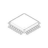
MC100EP195FAG ON Semiconductor, MC100EP195FAG Datasheet - Page 14

MC100EP195FAG
Manufacturer Part Number
MC100EP195FAG
Description
IC PROGRAM DELAY 3.3V ECL 32LQFP
Manufacturer
ON Semiconductor
Series
100EPr
Type
Programmable Delay Chipr
Datasheet
1.MC100EP195FAR2G.pdf
(20 pages)
Specifications of MC100EP195FAG
Input
ECL, LVCMOS, LVTTL
Output
ECL
Frequency - Max
1.2GHz
Voltage - Supply
3 V ~ 3.6 V
Operating Temperature
-40°C ~ 85°C
Mounting Type
Surface Mount
Package / Case
32-LQFP
Frequency-max
1.2GHz
Function
Active Programmable Delay Line
Supply Voltage (min)
+/- 3 V
Maximum Operating Temperature
+ 85 C
Minimum Operating Temperature
- 40 C
Mounting Style
SMD/SMT
Supply Voltage (max)
+/- 3.6 V
Lead Free Status / RoHS Status
Lead free / RoHS Compliant
Other names
MC100EP195FAGOS
Available stocks
Company
Part Number
Manufacturer
Quantity
Price
Company:
Part Number:
MC100EP195FAG
Manufacturer:
ON Semiconductor
Quantity:
10 000
Part Number:
MC100EP195FAG
Manufacturer:
ON/安森美
Quantity:
20 000
pictured in Figure 7. Use of this diagram will simplify the
explanation of how the cascade circuitry works. When D10
of chip #1 in Figure 6 is LOW this device’s
CASCADE output will also be low while the CASCADE
output will be high. In this condition the SET MIN pin of
chip #2 will be asserted HIGH and thus all of the latches of
chip #2 will be reset and the device will be set at its minimum
delay.
SET MAX deasserted so that its delay will be controlled
entirely by the address bus A0—A9. If the delay needed is
greater than can be achieved with 1023 gate delays
MAX
SET
SET
MIN
An expansion of the latch section of the block diagram is
Chip #1, on the other hand, will have both SET MIN and
D0 Q0
LEN
Set Reset
BIT 0
D1 Q1
LEN
Set Reset
BIT 1
Figure 7. Expansion of the Latch Section of the EP195 Block Diagram
D2 Q2
LEN
Set Reset
BIT 2
D3 Q3
LEN
Set Reset
BIT 3
TO SELECT MULTIPLEXERS
http://onsemi.com
D4 Q4
LEN
Set Reset
BIT 4
14
D5 Q5
LEN
Set Reset
BIT 5
(1111111111 on the A0—A9 address bus) D10 will be
asserted to signal the need to cascade the delay to the next
EP195 device. When D10 is asserted, the SET MIN pin of
chip #2 will be deasserted and SET MAX pin asserted
resulting in the device delay to be the maximum delay.
Table 13 shows the delay time of two EP195 chips in
cascade.
simply needs to connect the D10 pin from the next chip to
the address bus and CASCADE outputs to the next chip in
the same manner as pictured in Figure 6. The only addition
to the logic is the increase of one line to the address bus for
cascade control of the second programmable delay chip.
To expand this cascading scheme to more devices, one
D6 Q6
LEN
Set Reset
BIT 6
D7 Q7
LEN
Set Reset
BIT 7
D8 Q8
LEN
Set Reset
BIT 8
D9 Q9
LEN
Set Reset
BIT 9


