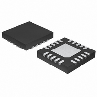
MAX3873AETP+T Maxim Integrated Products, MAX3873AETP+T Datasheet

MAX3873AETP+T
Specifications of MAX3873AETP+T
Related parts for MAX3873AETP+T
MAX3873AETP+T Summary of contents
Page 1
... CC QFN/TQFN** **NOTE: THE EXPOSED PAD MUST BE SOLDERED TO THE SUPPLY GROUND. ________________________________________________________________ Maxim Integrated Products For pricing, delivery, and ordering information, please contact Maxim Direct at 1-888-629-4642, or visit Maxim’s website at www.maxim-ic.com. ♦ Fully Integrated Clock Recovery and Data Retiming ♦ Power Dissipation: 260mW with +3.3V Supply ♦ ...
Page 2
Low-Power, Compact 2.5Gbps or 2.7Gbps Clock-Recovery and Data-Retiming IC ABSOLUTE MAXIMUM RATINGS Supply Voltage, V ..............................................-0.5V to +5.0V CC Voltage at SDI± .............................. (V CC CML Output Current at SDO±, SCLKO± ............................22mA Voltage at LOL, FASTRACK, FIL±, SCLKEN MODE, RATESET...................................-0.5V ...
Page 3
Low-Power, Compact 2.5Gbps or 2.7Gbps Clock-Recovery and Data-Retiming IC AC ELECTRICAL CHARACTERISTICS (V = 3.0V to 3.6V 0.022µ -40°C to +85°C. Typical values are noted.) (Note 4) PARAMETER SYMBOL Serial Input ...
Page 4
Low-Power, Compact 2.5Gbps or 2.7Gbps Clock-Recovery and Data-Retiming IC AC ELECTRICAL CHARACTERISTICS (continued 3.0V to 3.6V 0.022µ -40°C to +85°C. Typical values are noted.) (Note 4) Note 1: At ...
Page 5
Low-Power, Compact 2.5Gbps or 2.7Gbps Clock-Recovery and Data-Retiming +25°C, unless otherwise noted.) A RECOVERED CLOCK AND DATA (2.488Gbps 125mV/div RECOVERED CLOCK JITTER (2.488Gbps) JITTER TRANSFER 0.5 0 -0.5 -1.0 -1.5 BELLCORE MASK -2.0 -2.5 ...
Page 6
Low-Power, Compact 2.5Gbps or 2.7Gbps Clock-Recovery and Data-Retiming +25°C, unless otherwise noted.) A PULLIN RANGE (RATESET = 0) 3.0 2.9 2.8 2.7 2.6 2.5 2.4 2.3 2.2 2.1 2.0 -50 0 AMBIENT TEMPERATURE (°C) JITTER TOLERANCE vs. ...
Page 7
Low-Power, Compact 2.5Gbps or 2.7Gbps Clock-Recovery and Data-Retiming IC PIN NAME C l ock Outp ut E nab l e, TTL Inp ut. W hen S C LKE LKE ...
Page 8
Low-Power, Compact 2.5Gbps or 2.7Gbps Clock-Recovery and Data-Retiming IC The loop filter output controls the on-chip LC VCO run- ning at either 2.488GHz or 2.67GHz. The VCO provides low phase noise and is trimmed to the correct frequency. Clock jitter ...
Page 9
Low-Power, Compact 2.5Gbps or 2.7Gbps Clock-Recovery and Data-Retiming IC Sinusoidal Jitter Tolerance and Input Deterministic Jitter Trade-Offs The MAX3873A has excellent jitter tolerance. Adding DJ to the input will close the eye opening and result in reduced sinusoidal jitter tolerance. ...
Page 10
... Maxim cannot assume responsibility for use of any circuitry other than circuitry entirely embodied in a Maxim product. No circuit patent licenses are implied. Maxim reserves the right to change the circuitry and specifications without notice at any time. 10 _____________________________Maxim Integrated Products, 120 San Gabriel Drive, Sunnyvale, CA 94086 408-737-7600 © 2007 Maxim Integrated Products ...


