ICS8312AYILF IDT, Integrated Device Technology Inc, ICS8312AYILF Datasheet
ICS8312AYILF
Specifications of ICS8312AYILF
Available stocks


Related parts for ICS8312AYILF


ICS8312AYILF Summary of contents
Page 1
LOW SKEW, 1-TO-12 LVCMOS/LVTTL FANOUT BUFFER General Description The ICS8312I is a low skew, 1-to-12 LVCMOS/ ICS LVTTL Fanout Buffer and a member of the HiPerClockS™ family of High Performance Clock HiPerClockS™ Solutions from IDT. The ICS8312I single-ended clock input ...
Page 2
ICS8312I LOW SKEW, 1-TO-12 LVCMOS/LVTTL FANOUT BUFFER Table 1. Pin Descriptions Number Name 12, 16, GND 17, 21, 25 CLK_EN 4 CLK 11, 13, 15, Q11, Q10, Q9, ...
Page 3
ICS8312I LOW SKEW, 1-TO-12 LVCMOS/LVTTL FANOUT BUFFER Function Tables Table 3A. Output Enable and Clock Enable Function Table Inputs OE CLK_EN Follows CLK input Table 3B. Output Enable and Clock Enable Function Table Inputs ...
Page 4
ICS8312I LOW SKEW, 1-TO-12 LVCMOS/LVTTL FANOUT BUFFER Absolute Maximum Ratings NOTE: Stresses beyond those listed under Absolute Maximum Ratings may cause permanent damage to the device. These ratings are stress specifications only. Functional operation of product at these conditions or ...
Page 5
ICS8312I LOW SKEW, 1-TO-12 LVCMOS/LVTTL FANOUT BUFFER Table 4D. Power Supply DC Characteristics, V Symbol Parameter V Positive Supply Voltage DD V Output Supply Voltage DDO I Power Supply Current DD I Output Supply Current DDO Table 4E. Power Supply ...
Page 6
ICS8312I LOW SKEW, 1-TO-12 LVCMOS/LVTTL FANOUT BUFFER Table 4G. LVCMOS/LVTTL DC Characteristics, T Symbol Parameter V Input High Voltage IH V Input Low Voltage IL CLK Input I IH High Current OE, CLK_EN CLK Input I IL Low Current OE, ...
Page 7
ICS8312I LOW SKEW, 1-TO-12 LVCMOS/LVTTL FANOUT BUFFER AC Electrical Characteristics Table 5A. AC Characteristics, V Parameter Symbol f Output Frequency MAX tp Propagation Delay, Low to High; NOTE 1 LH Buffer Additive Phase Jitter, RMS; refer to tjit Additive Phase ...
Page 8
ICS8312I LOW SKEW, 1-TO-12 LVCMOS/LVTTL FANOUT BUFFER Table 5C. AC Characteristics, V Parameter Symbol f Output Frequency MAX tp Propagation Delay, Low to High; NOTE 1 LH Buffer Additive Phase Jitter, RMS; refer to tjit Additive Phase Jitter Section tsk(o) ...
Page 9
ICS8312I LOW SKEW, 1-TO-12 LVCMOS/LVTTL FANOUT BUFFER Table 5E. AC Characteristics, V Parameter Symbol f Output Frequency MAX tp Propagation Delay, Low to High; NOTE 1 LH Buffer Additive Phase Jitter, RMS; refer to tjit Additive Phase Jitter Section tsk(o) ...
Page 10
ICS8312I LOW SKEW, 1-TO-12 LVCMOS/LVTTL FANOUT BUFFER Additive Phase Jitter The spectral purity in a band at a specific offset from the fundamental compared to the power of the fundamental is called the dBc Phase Noise. This value is normally ...
Page 11
ICS8312I LOW SKEW, 1-TO-12 LVCMOS/LVTTL FANOUT BUFFER Parameter Measurement Information 1.65V±5% V DD, V DDO LVCMOS GND -1.65V±5% 3.3V Core/3.3V LVCMOS Output Load AC Test Circuit 0.9V±0.1V V DD, V DDO LVCMOS GND -0.9V±0.1V 1.8V Core/1.8V LVCMOS Output Load AC ...
Page 12
ICS8312I LOW SKEW, 1-TO-12 LVCMOS/LVTTL FANOUT BUFFER Parameter Measurement Information, continued V DDO DDO Qy 2 tsk(o) Output Skew CLK V DDO Q0:Q11 Propagation Delay 80% 20% Q0:Q11 t R Output ...
Page 13
ICS8312I LOW SKEW, 1-TO-12 LVCMOS/LVTTL FANOUT BUFFER Application Information Recommendations for Unused Input and Output Pins Inputs: LVCMOS Control Pins: All control pins have internal pull-ups or pull-downs; additional resistance is not required but can be added for additional protection. ...
Page 14
ICS8312I LOW SKEW, 1-TO-12 LVCMOS/LVTTL FANOUT BUFFER Reliability Information θ Table 6. vs. Air Flow Table for a 32 Lead LQFP JA Linear Feet per Minute Single-Layer PCB, JEDEC Standard Test Boards Multi-Layer PCB, JEDEC Standard Test Boards NOTE: Most ...
Page 15
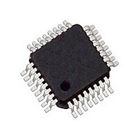
ICS8312I LOW SKEW, 1-TO-12 LVCMOS/LVTTL FANOUT BUFFER Package Outline and Package Dimensions Package Outline - Y Suffix for 32 Lead LQFP Table 7. Package Dimensions for 32 Lead LQFP JEDEC Variation: ABC - HD All Dimensions in Millimeters Symbol Minimum ...
Page 16
... ICS8312AYILF 8312AYILFT ICS8312AYILF NOTE: Parts that are ordered with an "LF" suffix to the part number are the Pb-Free configuration and are RoHS compliant. While the information presented herein has been checked for both accuracy and reliability, Integrated Device Technology (IDT) assumes no responsibility for either its use or for the infringement of any patents or other rights of third parties, which would result from its use ...
Page 17
ICS8312I LOW SKEW, 1-TO-12 LVCMOS/LVTTL FANOUT BUFFER Revision History Sheet Rev Table Page T5A - T5F IDT™ / ICS™ LVCMOS/LVTTL FANOUT BUFFER Description of Change Features section - added lead-free ...
Page 18
ICS8312I LOW SKEW, 1-TO-12 LVCMOS/LVTTL FANOUT BUFFER Contact Information: www.IDT.com Sales 800-345-7015 (inside USA) +408-284-8200 (outside USA) Fax: 408-284-2775 www.IDT.com/go/contactIDT © 2008 Integrated Device Technology, Inc. All rights reserved. Product specifications subject to change without notice. IDT and the IDT ...