NB7VQ58MMNG ON Semiconductor, NB7VQ58MMNG Datasheet
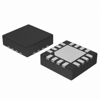
IC CLOCK/DATA MULTIPLEXER 16QFN

NB7VQ58MMNG

Manufacturer Part Number
NB7VQ58MMNG
Description
IC CLOCK/DATA MULTIPLEXER 16QFN
Manufacturer
ON Semiconductor
Series
GigaComm™r
Type
Multiplexer , Datar
Datasheet

Specifications of NB7VQ58MMNG

Number Of Circuits
1
Ratio - Input:output
2:1
Differential - Input:output
Yes/Yes
Input
CML, LVDS, LVPECL
Output
CML
Frequency - Max
7GHz
Voltage - Supply
1.71 V ~ 3.6 V
Operating Temperature
-40°C ~ 85°C
Mounting Type
Surface Mount
Package / Case
16-TFQFN Exposed Pad
Frequency-max
7GHz
Lead Free Status / RoHS Status
Lead free / RoHS Compliant
NB7VQ58M
1.8V / 2.5V / 3.3V
Differential 2:1 Clock/Data
Multiplexer / Translator
with CML Outputs
w/ Selectable Input Equalizer
Multi−Level Inputs w/ Internal Termination
Description
Data multiplexer with a selectable Equalizer receiver. When placed in
series with a Clock /Data path operating up to 7 GHz or 10.7 Gb/s,
respectively, the NB7VQ58M inputs will compensate the degraded
signal transmitted across an FR4 PCB backplane or cable
interconnect. Therefore, the serial data rate is increased by reducing
Inter−Symbol Interference (ISI) caused by losses in copper
interconnect or long cables.
either flow through or bypass the Equalizer section. Control of the
Equalizer function is realized by setting EQEN; When EQEN is set
Low, the INn / INn inputs bypass the Equalizer. When EQEN is set
High, the INn / INn inputs flow through the Equalizer. The default
state at startup is LOW. As such, the NB7VQ58M is ideal for SONET,
GigE, Fiber Channel, Backplane and other Clock/Data distribution
applications.
resistors that are accessed through the VT pin. This feature allows the
NB7VQ58M to accept various logic level standards, such as LVPECL,
CML or LVDS.
up to 7 GHz or 10.7 Gb/s, respectively.
50 W terminations and 400 mV output swings when externally
terminated with a 50 W resistor to V
QFN package and is a member of the GigaComm™ family of high
performance Clock / Data products. Application notes, models, and
support documentation are available at www.onsemi.com.
Features
© Semiconductor Components Industries, LLC, 2009
August, 2009 − Rev. 0
The NB7VQ58M is a high performance differential 2−to−1 Clock or
The EQualizer ENable pin (EQEN) allows the INn/INn inputs to
The differential inputs incorporate internal 50 W termination
The NB7VQ58M produces minimal Clock or Data jitter operating
The 16 mA differential CML outputs provide matching internal
The NB7VQ58M is offered in a low profile 3mm x 3 mm 16−pin
Maximum Input Clock Frequency > 7 GHz
Random Clock Jitter < 0.8 ps RMS
Selectable Input Equalization
180 ps Typical Propagation Delay
35 ps Typical Rise and Fall Times
Maximum Input Data Rate > 10.7 Gb/s
Data Dependent Jitter < 15 ps
CC
.
1
Differential CML Outputs, 400 mV Peak−to−Peak,
Typical
Operating Range: V
0 V
Internal 50 W Input Termination Resistors
This is a Pb−Free Device
See detailed ordering and shipping information in the package
dimensions section on page 8 of this data sheet.
*For additional marking information, refer to
CASE 485G
MN SUFFIX
(Note: Microdot may be in either location)
Application Note AND8002/D.
QFN−16
SIMPLIFIED BLOCK DIAGRAM
1
ORDERING INFORMATION
A
L
Y
W
G
V
CC
CC
http://onsemi.com
= 1.71 V to 3.6 V with GND =
= Assembly Location
= Wafer Lot
= Year
= Work Week
= Pb−Free Package
Publication Order Number:
1
DIAGRAM*
16
MARKING
EQ
ALYW G
Q58M
NB7V
G
NB7VQ58M/D

Related parts for NB7VQ58MMNG

NB7VQ58MMNG Summary of contents

Page 1

NB7VQ58M 1.8V / 2.5V / 3.3V Differential 2:1 Clock/Data Multiplexer / Translator with CML Outputs w/ Selectable Input Equalizer Multi−Level Inputs w/ Internal Termination Description The NB7VQ58M is a high performance differential 2−to−1 Clock or Data multiplexer with a selectable ...

Page 2

VT0 GND GND VCC IN0 1 2 IN0 NB7VQ58M IN1 3 IN1 VT1 SEL EQEN VCC Figure 1. Pin Configuration Table 1. EQualizer ENable FUNCTION EQEN Function 0 INn / INn ...

Page 3

Table 4. ATTRIBUTES ESD Protection R − SEL Input Pull−up Resistor PU Moisture Sensitivity (Note 3) Flammability Rating Transistor Count Meets or exceeds JEDEC Spec EIA/JESD78 IC Latchup Test 3. For additional information, see Application Note AND8003/D. Table 5. MAXIMUM ...

Page 4

Table 6. DC CHARACTERISTICS POSITIVE CML OUTPUT Symbol POWER SUPPLY CURRENT I Power Supply Current (Inputs and Outputs Open) CC CML OUTPUTS (Note 6) V Output HIGH Voltage OH V Output LOW Voltage OL DIFFERENTIAL INPUTS DRIVEN SINGLE−ENDED (Note 7) ...

Page 5

Table 7. AC CHARACTERISTICS (V Symbol f Maximum Input Clock Frequency MAX f Maximum Operating Data Rate (PRBS23) DATAMAX fSEL Maximum Toggle Frequency, SEL V Output Voltage Amplitude EQEN = OUTPP (Note 12) (Figures 3 and 11) ...

Page 6

Figure 6. Differential Input Driven Single−Ended IHmax V thmax V ILmax IHmin V thmin V ILmin GND Figure ...

Page 7

Driver Q Q DJ1 Figure 12. Typical NB7VQ58M Equalizer Application and Interconnect with PRBS23 pattern at 6.5 Gbps, EQEN = FR4 − 12 Inch Backplane IN IN DJ2 http://onsemi.com 7 NB7VQ58M EQualizer EQEN = 1 DJ3 ...

Page 8

... Figure 15. Standard 50 W Load CML Interface 50 W Figure 17. Typical CML Output Structure and Termination ORDERING INFORMATION Device NB7VQ58MMNG NB7VQ58MMNHTBG NB7VQ58MMNTXG †For information on tape and reel specifications, including part orientation and tape sizes, please refer to our Tape and Reel Packaging Specifications Brochure, BRD8011/D. ...

Page 9

... E2 3.25 e 0.128 *For additional information on our Pb−Free strategy and soldering details, please download the ON Semiconductor Soldering and Mounting Techniques Reference Manual, SOLDERRM/D. N. American Technical Support: 800−282−9855 Toll Free USA/Canada Europe, Middle East and Africa Technical Support: Phone: 421 33 790 2910 Japan Customer Focus Center Phone: 81− ...

Related keywords