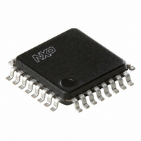
PCK9447BD,157 NXP Semiconductors, PCK9447BD,157 Datasheet

PCK9447BD,157
Specifications of PCK9447BD,157
935280283157
PCK9447BD
Available stocks
Related parts for PCK9447BD,157
PCK9447BD,157 Summary of contents
Page 1
PCK9447 3.3 V/2 LVCMOS clock fan-out buffer Rev. 01 — 13 October 2005 1. General description The PCK9447 2.5 V compatible clock fan-out buffer targeted for high performance ...
Page 2
Philips Semiconductors 3. Ordering information Table 1: Type number PCK9447BD 4. Functional diagram Fig 1. Functional diagram of PCK9447 9397 750 12522 Product data sheet Ordering information Package Name Description LQFP32 plastic low profile quad flat package; 32 leads; body ...
Page 3
Philips Semiconductors 5. Pinning information 5.1 Pinning Fig 2. Pin configuration for LQFP32 5.2 Pin description Table 2: Symbol CCLK0 CCLK1 CLK_SEL CLK_STOP GND V CC 9397 750 12522 Product data sheet GND 1 2 CLK_SEL ...
Page 4
Philips Semiconductors 6. Functional description 6.1 Function table Table 3: Control CLK_SEL OE CLK_STOP [ will high-impedance 3-state all outputs independent of CLK_STOP. 7. Limiting values Table 4: In accordance with the Absolute Maximum Rating System (IEC ...
Page 5
Philips Semiconductors 8.2 Static characteristics Table 6: Static characteristics (3 + 3.3 V amb CC Symbol Parameter V HIGH-state input voltage IH V LOW-state input voltage IL V HIGH-state output voltage ...
Page 6
Philips Semiconductors 8.3 Dynamic characteristics Table 8: Dynamic characteristics (3 + 3.3 V amb CC Symbol Parameter f input frequency i f output frequency o t reference input pulse width W(i)(ref) ...
Page 7
Philips Semiconductors Table 9: Dynamic characteristics (2 + 2.5 V amb CC Symbol Parameter f input frequency i f output frequency o t reference input pulse width W(i)(ref ...
Page 8
Philips Semiconductors CCLK Fig 5. Propagation delay (t ) test reference PD t sk(o) The pin-to-pin skew is defined as the worst-case difference in propagation delay between any similar delay path within a single device. Fig 7. ...
Page 9
Philips Semiconductors 9. Application information 9.1 Driving transmission lines The PCK9447 clock driver was designed to drive high-speed signals in a terminated transmission line environment. To provide the optimum flexibility to the user the output drivers were designed to exhibit ...
Page 10
Philips Semiconductors 3 the load end the voltage will double, due to the near unity reflection coefficient will then increment ...
Page 11
Philips Semiconductors 10. Test information Fig 14. CCLK AC test reference for V 9397 750 12522 Product data sheet 3.3 V/2 LVCMOS clock fan-out buffer PCK9447 D.U. PULSE GENERATOR ...
Page 12
Philips Semiconductors 11. Package outline LQFP32: plastic low profile quad flat package; 32 leads; body 1 pin 1 index DIMENSIONS (mm are the original dimensions) ...
Page 13
Philips Semiconductors 12. Soldering 12.1 Introduction to soldering surface mount packages This text gives a very brief insight to a complex technology. A more in-depth account of soldering ICs can be found in our Data Handbook IC26; Integrated Circuit Packages ...
Page 14
Philips Semiconductors – smaller than 1.27 mm, the footprint longitudinal axis must be parallel to the transport direction of the printed-circuit board. The footprint must incorporate solder thieves at the downstream end. • For packages with leads on four sides, ...
Page 15
Philips Semiconductors [3] These transparent plastic packages are extremely sensitive to reflow soldering conditions and must on no account be processed through more than one soldering cycle or subjected to infrared reflow soldering with peak temperature exceeding 217 C body ...
Page 16
Philips Semiconductors 15. Data sheet status [1] Level Data sheet status Product status I Objective data Development II Preliminary data Qualification III Product data Production [1] Please consult the most recently issued data sheet before initiating or completing a design. ...
Page 17
Philips Semiconductors 20. Contents 1 General description . . . . . . . . . . . . . . . . . . . . . . 1 2 Features . . . . . . . . ...


