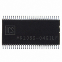
MK2069-04GILF IDT, Integrated Device Technology Inc, MK2069-04GILF Datasheet - Page 9

MK2069-04GILF
Manufacturer Part Number
MK2069-04GILF
Description
IC CLOCK SYNTHESIZER 56-TSSOP
Manufacturer
IDT, Integrated Device Technology Inc
Type
Clock Synchronizerr
Datasheet
1.MK2069-04GILF.pdf
(20 pages)
Specifications of MK2069-04GILF
Pll
Yes
Input
LVCMOS
Output
LVCMOS
Number Of Circuits
1
Ratio - Input:output
1:3
Differential - Input:output
No/No
Frequency - Max
160MHz
Divider/multiplier
Yes/No
Voltage - Supply
3.15 V ~ 3.45 V
Operating Temperature
-40°C ~ 85°C
Mounting Type
Surface Mount
Package / Case
56-TSSOP
Frequency-max
160MHz
Number Of Elements
2
Supply Current
30mA
Pll Input Freq (min)
1KHz
Pll Input Freq (max)
170MHz
Operating Supply Voltage (typ)
3.3V
Operating Temp Range
-40C to 85C
Package Type
TSSOP
Output Frequency Range
0.5 to 160MHz
Operating Supply Voltage (min)
3.15V
Operating Supply Voltage (max)
3.45V
Operating Temperature Classification
Industrial
Pin Count
56
Lead Free Status / RoHS Status
Lead free / RoHS Compliant
Other names
800-1783
800-1783-5
800-1783
800-1783-5
800-1783
Available stocks
Company
Part Number
Manufacturer
Quantity
Price
Company:
Part Number:
MK2069-04GILF
Manufacturer:
IDT Integrated Device Technolo
Quantity:
135
Company:
Part Number:
MK2069-04GILF
Manufacturer:
Vishay
Quantity:
2 489
Company:
Part Number:
MK2069-04GILFTR
Manufacturer:
TEMIC
Quantity:
36 603
Part Number:
MK2069-04GILFTR
Manufacturer:
ICS
Quantity:
20 000
Loop Filter Capacitor Type
Loop filters must use specific types of capacitors.
Recommendations for these capacitors can be found at
www.idt.com/?app=calculators&source=support_menu.
Input Phase Compensation Circuit
The VCXO PLL includes a special input clock phase
compensation circuit. It is used when changing the phase of
the input clock, which might occur when selecting a new
reference input through the use of an external clock
multiplexer.
The phase compensation circuit allows the VCXO PLL to
quickly lock to the new input clock phase without producing
extra clock cycles or clock wander, assuming the new clock
is at the same frequency.
Input pin CLR controls the phase compensation circuit. CLR
must remain high for normal operation. When used in
conjunction with an external multiplexer (MUX), CLR should
be brought low prior to MUX reselection, then returned high
after MUX reselection. This prevents the VCXO PLL from
attempting to lock to the new input clock phase associated
with the input clock.
When CLR is high, the VCXO PLL operates normally.
When CLR is low, the VCXO PLL charge pump output is
inactivated which means that no charge pump correction
pulses are provided to the loop filter. During this time, the
VCXO frequency is held constant by the residual charge or
voltage on the PLL loop filter, regardless of the input clock
condition. However, the VCXO frequency will drift over time,
eventually to the minimum pull range of the crystal, due to
leak-off of the loop filter charge. This means that CLR can
provide a holdover function, but only for a very short
duration, typically in milliseconds.
IDT® VCXO-BASED UNIVERSAL CLOCK TRANSLATOR
MK2069-04
VCXO-BASED UNIVERSAL CLOCK TRANSLATOR
output generated with the VCXO PLL configuration will be OC-3 and OC-12 timing jitter compliant.
2) This is a reduced cost and size variant of the above filter, due to the decreased size of C
GR-1244-CORE compliance is not needed.
3) This configuration is used to generate a DS3 clock of 44.768 MHz at the TCLK output. This configuration is
GR-1244-CORE compliant when used following a system synchronizer.
4) Lowering the phase detector frequency, by increasing the value of the RPV and/or RV dividers and the FV divider,
will lower the loop bandwidth and/or decrease the size of C
9
Upon bringing CLR high, the FV Divider is reset and begins
counting upon with the first positive edge of the new input
clock, and the charge pump is re-activated. By resetting the
FV Divider, the memory of the previous input clock phase is
removed from the feedback divider, eliminating the
generation of extra VCLK clock cycles that would occur if the
loop was to re-lock under normal means. Lock time is also
reduced, as is the generation of clock wander.
By using CLR in this fashion VCLK will align to the input
clock phase with only one or two VCLK cycle slips resulting.
When CLR is not used, the number of VCLK cycle slips can
be as high the FV Divider value.
TCLK is always locked to VCLK regardless of the state of
the CLR input.
Lock Detection
The MK2069-04 includes a lock detection feature that
indicates lock status of VCLK relative to the selected input
reference clock. When phase lock is achieved (such as
following power-up), the LD output goes high. When phase
lock is lost (such as when the input clock stops, drifts beyond
the pullable range of the crystal, or suddenly shifts in
phase), the LD output goes low.
The definition of a “locked” condition is determined by the
user. LD is high when the VCXO PLL phase detector error
is below the user-defined threshold. This threshold is set by
external components RLD and CLD shown in the Lock
Detection Circuit Diagram, below.
To help guard against false lock indications, the LD pin will
go high only when the phase error is below the set threshold
for 8 consecutive phase detector cycles. The LD pin will go
low when the phase error is above the set threshold for only
1 phase detector cycle.
The lock detector threshold (phase error) is determined by
S
for the same damping factor.
VCXO AND SYNTHESIZER
S
. It is useful when
MK2069-04
REV J 051310


