MM74HC4046M Fairchild Semiconductor, MM74HC4046M Datasheet

IC LOCK LOOP PHASE CMOS 16-SOIC

MM74HC4046M

Manufacturer Part Number
MM74HC4046M
Description
IC LOCK LOOP PHASE CMOS 16-SOIC
Manufacturer
Fairchild Semiconductor
Series
74HCr
Type
Phase Lock Loop (PLL)r
Datasheet

Specifications of MM74HC4046M

Pll
No
Input
CMOS
Output
3-State
Number Of Circuits
1
Ratio - Input:output
1:2
Differential - Input:output
No/No
Frequency - Max
14MHz
Divider/multiplier
No/No
Voltage - Supply
2 V ~ 6 V
Operating Temperature
-40°C ~ 85°C
Mounting Type
Surface Mount
Package / Case
16-SOIC (3.9mm Width)
Frequency-max
14MHz
Supply Voltage (max)
6 V
Supply Voltage (min)
2 V
Maximum Operating Temperature
+ 85 C
Minimum Operating Temperature
- 40 C
Mounting Style
SMD/SMT
Operating Supply Voltage
2 V to 6 V
Number Of Elements
1
Operating Supply Voltage (typ)
2.5/3.3/5V
Operating Temp Range
-40C to 85C
Package Type
SOIC N
Operating Supply Voltage (min)
2V
Operating Supply Voltage (max)
6V
Operating Temperature Classification
Industrial
Pin Count
16
Pll Type
Frequency Synthesis
Frequency
14MHz
Supply Current
600µA
Supply Voltage Range
2V To 6V
Digital Ic Case Style
SOIC
No. Of Pins
16
Operating Temperature Range
-40°C To +85°C
Rohs Compliant
Yes
Lead Free Status / RoHS Status
Lead free / RoHS Compliant

Available stocks

Company
Part Number
Manufacturer
Quantity
Price
Part Number:
MM74HC4046M
Manufacturer:
FAIRCHIL
Quantity:
222
© 2003 Fairchild Semiconductor Corporation
MM74HC4046M
MM74HC4046SJ
MM74HC4046MTC
MM74HC4046N
MM74HC4046
CMOS Phase Lock Loop
General Description
The MM74HC4046 is a low power phase lock loop utilizing
advanced silicon-gate CMOS technology to obtain high fre-
quency operation both in the phase comparator and VCO
sections. This device contains a low power linear voltage
controlled oscillator (VCO), a source follower, and three
phase comparators. The three phase comparators have a
common signal input and a common comparator input. The
signal input has a self biasing amplifier allowing signals to
be either capacitively coupled to the phase comparators
with a small signal or directly coupled with standard input
logic levels. This device is similar to the CD4046 except
that the Zener diode of the metal gate CMOS device has
been replaced with a third phase comparator.
Phase Comparator I is an exclusive OR (XOR) gate. It pro-
vides a digital error signal that maintains a 90 phase shift
between the VCO’s center frequency and the input signal
(50% duty cycle input waveforms). This phase detector is
more susceptible to locking onto harmonics of the input fre-
quency than phase comparator I, but provides better noise
rejection.
Phase comparator III is an SR flip-flop gate. It can be used
to provide the phase comparator functions and is similar to
the first comparator in performance.
Phase comparator II is an edge sensitive digital sequential
network. Two signal outputs are provided, a comparator
output and a phase pulse output. The comparator output is
a 3-STATE output that provides a signal that locks the VCO
output signal to the input signal with 0 phase shift between
Ordering Code:
Devices also available in Tape and Reel. Specify by appending the suffix letter “X” to the ordering code.
Order Number
Package Number
MTC16
M16A
M16D
N16E
16-Lead Small Outline Integrated Circuit (SOIC), JEDEC MS-012, 0.150" Narrow
16-Lead Small Outline Package (SOP), EIAJ TYPE II, 5.3mm Wide
16-Lead Thin Shrink Small Outline Package (TSSOP), JEDEC MO-153, 4.4mm Wide
16-Lead Plastic Dual-In-Line Package (PDIP), JEDEC MS-001, 0.300" Wide
DS005352
them. This comparator is more susceptible to noise throw-
ing the loop out of lock, but is less likely to lock onto har-
monics than the other two comparators.
In a typical application any one of the three comparators
feed an external filter network which in turn feeds the VCO
input. This input is a very high impedance CMOS input
which also drives the source follower. The VCO’s operating
frequency is set by three external components connected
to the C1A, C1B, R1 and R2 pins. An inhibit pin is provided
to disable the VCO and the source follower, providing a
method of putting the IC in a low power state.
The source follower is a MOS transistor whose gate is con-
nected to the VCO input and whose drain connects the
Demodulator output. This output normally is used by tying
a resistor from pin 10 to ground, and provides a means of
looking at the VCO input without loading down modifying
the characteristics of the PLL filter.
Features
Low dynamic power consumption:
Maximum VCO operating frequency:
12 MHz (V
Fast comparator response time (V
VCO has high linearity and high temperature stability
Comparator I:
Comparator II:
Comparator III: 25 ns
Package Description
CC
4.5V)
25 ns
30 ns
February 1984
Revised October 2003
CC
(V
www.fairchildsemi.com
CC
4.5V)
4.5V)

Related parts for MM74HC4046M

MM74HC4046M Summary of contents

Page 1

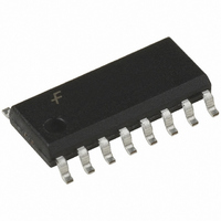
... M16A 16-Lead Small Outline Integrated Circuit (SOIC), JEDEC MS-012, 0.150" Narrow MM74HC4046SJ M16D 16-Lead Small Outline Package (SOP), EIAJ TYPE II, 5.3mm Wide MM74HC4046MTC MTC16 16-Lead Thin Shrink Small Outline Package (TSSOP), JEDEC MO-153, 4.4mm Wide MM74HC4046N N16E 16-Lead Plastic Dual-In-Line Package (PDIP), JEDEC MS-001, 0.300" Wide Devices also available in Tape and Reel. Specify by appending the suffix letter “ ...

Page 2

Connection Diagram Pin Assignments for DIP, SOIC, SOP and TSSOP Block Diagram www.fairchildsemi.com 2 ...

Page 3

Absolute Maximum Ratings (Note 2) Supply Voltage ( Input Voltage ( Output Voltage ( OUT Clamp Diode Current ( Output Current per pin (I ...

Page 4

AC Electrical Characteristics Symbol Parameters Conditions AC Coupled C (series) Input Sensitivity, f 500 kHz IN Signal Maximum Output r f Rise and Fall Time C Maximum Input Capacitance IN Phase Comparator ...

Page 5

Typical Performance Characteristics Typical Center Frequency vs R1 4.5V CC Typical Offset Frequency vs R2 4.5V CC Typical VCO Power Dissipation @ Center Frequency vs R1 Typical Center Frequency vs R1 Typical ...

Page 6

Typical Performance Characteristics VCO 4.5V in out CC VCO vs out Temperature V 4.5V CC www.fairchildsemi.com (Continued) VCO 4.5V in out CC VCO vs out Temperature ...

Page 7

Typical Performance Characteristics HC4046 Typical Source Follower Power Dissipation vs RS Typical VCO Linaearity vs R1 & C1 (Continued) Typical R2/R1 MAX MIN V 4.5V & MAX MIN Typical VCO Linearity vs R1 ...

Page 8

Detailed Circuit Description VOLTAGE CONTROLLED OSCILLATOR/SOURCE FOLLOWER The VCO requires two or three external components to operate. These are R1, R2, C1. Resistor R1 and capacitor C1 are selected to determine the center frequency of the VCO. R1 controls the ...

Page 9

Detailed Circuit Description FIGURE 2. Logic Diagram for VCO The input to the VCO is a very high impedance CMOS input and so it will not load down the loop filter, easing the filters design. In order to make signals ...

Page 10

Detailed Circuit Description FIGURE 4. Typical Phase Comparator I. Waveforms Thus in normal operation V and ground voltage levels CC are fed to the loop filter. This differs from some phase detectors which supply a current output to the loop ...

Page 11

Detailed Circuit Description Phase Comparator State Diagrams (Continued) FIGURE 5. PLL State Tables 11 www.fairchildsemi.com ...

Page 12

Detailed Circuit Description FIGURE 6. Logic Diagram for Phase Comparator II FIGURE 7. Typical Phase Comparator II Output Waveforms www.fairchildsemi.com (Continued) 12 ...

Page 13

Detailed Circuit Description If the VCO leads the signal then when the leading edge of the VCO is seen the output of the phase comparator goes LOW. This discharges the loop filter until the leading edge of the signal is ...

Page 14

Physical Dimensions inches (millimeters) unless otherwise noted 16-Lead Small Outline Integrated Circuit (SOIC), JEDEC MS-012, 0.150" Narrow www.fairchildsemi.com Package Number M16A 14 ...

Page 15

Physical Dimensions inches (millimeters) unless otherwise noted (Continued) 16-Lead Small Outline Package (SOP), EIAJ TYPE II, 5.3mm Wide Package Number M16D 15 www.fairchildsemi.com ...

Page 16

Physical Dimensions inches (millimeters) unless otherwise noted (Continued) 16-Lead Thin Shrink Small Outline Package (TSSOP), JEDEC MO-153, 4.4mm Wide www.fairchildsemi.com Package Number MTC16 16 ...

Page 17

Physical Dimensions inches (millimeters) unless otherwise noted (Continued) 16-Lead Plastic Dual-In-Line Package (PDIP), JEDEC MS-001, 0.300" Wide Fairchild does not assume any responsibility for use of any circuitry described, no circuit patent licenses are implied and Fairchild reserves the right ...

Related keywords