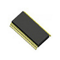
MK2069-03GI IDT, Integrated Device Technology Inc, MK2069-03GI Datasheet - Page 10

MK2069-03GI
Manufacturer Part Number
MK2069-03GI
Description
IC VCXO CLK TRANSLATOR 56-TSSOP
Manufacturer
IDT, Integrated Device Technology Inc
Type
Clock Synchronizerr
Datasheet
1.MK2069-03GITR.pdf
(20 pages)
Specifications of MK2069-03GI
Pll
Yes
Input
LVCMOS
Output
LVCMOS
Number Of Circuits
1
Ratio - Input:output
1:3
Differential - Input:output
No/No
Frequency - Max
160MHz
Divider/multiplier
Yes/No
Voltage - Supply
3.15 V ~ 3.45 V
Operating Temperature
-40°C ~ 85°C
Mounting Type
Surface Mount
Package / Case
56-TSSOP
Frequency-max
160MHz
Number Of Elements
2
Supply Current
30mA
Pll Input Freq (min)
1KHz
Pll Input Freq (max)
27MHz
Operating Supply Voltage (typ)
3.3V
Operating Temp Range
-40C to 85C
Package Type
TSSOP
Output Frequency Range
2.5 to 160MHz
Operating Supply Voltage (min)
3.15V
Operating Supply Voltage (max)
3.45V
Operating Temperature Classification
Industrial
Pin Count
56
Lead Free Status / RoHS Status
Contains lead / RoHS non-compliant
Under ideal conditions, where the VCXO is phase- locked to
a low-jitter reference input, loop phase error is typically
maintained to within a few nanoseconds.
Lock Detection Circuit Diagram
If the lock detection circuit is not used, the LDR output may
remain unconnected, however the LDC input should be tied
high or low. If the PCB was designed to accommodate the
RLD and CLD components but the LD output will not be
used, RLD can remain unstuffed and CLD can be replaced
with a resistor (< 10 kohm).
Power Supply Considerations
As with any integrated clock device, the MK2069-03 has a
special set of power supply requirements:
•
IDT™ / ICS™ VCXO-BASED CLOCK TRANSLATOR WITH HIGH MULTIPLICATION 10
MK2069-03
VCXO-BASED CLOCK TRANSLATOR WITH HIGH MULTIPLICATION
The feed from the system power supply must be filtered
for noise that can cause output clock jitter. Power supply
noise sources include the system switching power supply
or other system components. The noise can interfere with
device PLL components such as the VCO or phase
detector.
D e te c to r
D iv id e r
O u tp u t
O u tp u t
P h a s e
V C X O
E rro r
F V
C L D
L o c k D e te ctio n C irc u it
R L D
L D R
(8 u p , 1 d o w n )
Q u a lific a tio n
L D C
C o u n te r
L o c k
R E S E T
In p u t T h res h o ld
se t to V D D /2
L D
O E L
•
•
This above set of requirements is served by the circuit
illustrated in the Recommended Power Supply Connection
(next page). The main features of this circuit are as follows:
•
•
•
•
Each VDD pin must be decoupled individually to prevent
power supply noise generated by one device circuit block
from interfering with another circuit block.
Clock noise from device VDD pins must not get onto the
PCB power plane or system EMI problems may result.
Only one connection is made to the PCB power plane.
The capacitors and ferrite chip (or ferrite bead) on the
common device supply form a lowpass ‘pi’ filter that
remove noise from the power supply as well as clock
noise back toward the supply. The bulk capacitor should
be a tantalum type, 1 F minimum. The other capacitors
should be ceramic type.
The power supply traces to the individual VDD pins
should fan out at the common supply filter to reduce
interaction between the device circuit blocks.
The decoupling capacitors at the VDD pins should be
ceramic type and should be as close to the VDD pin as
possible. There should be no via’s between the
decoupling capacitor and the supply pin.
VCXO AND SYNTHESIZER
MK2069-03
REV J 030906


