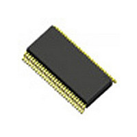
MK2069-03GI IDT, Integrated Device Technology Inc, MK2069-03GI Datasheet - Page 6

MK2069-03GI
Manufacturer Part Number
MK2069-03GI
Description
IC VCXO CLK TRANSLATOR 56-TSSOP
Manufacturer
IDT, Integrated Device Technology Inc
Type
Clock Synchronizerr
Datasheet
1.MK2069-03GITR.pdf
(20 pages)
Specifications of MK2069-03GI
Pll
Yes
Input
LVCMOS
Output
LVCMOS
Number Of Circuits
1
Ratio - Input:output
1:3
Differential - Input:output
No/No
Frequency - Max
160MHz
Divider/multiplier
Yes/No
Voltage - Supply
3.15 V ~ 3.45 V
Operating Temperature
-40°C ~ 85°C
Mounting Type
Surface Mount
Package / Case
56-TSSOP
Frequency-max
160MHz
Number Of Elements
2
Supply Current
30mA
Pll Input Freq (min)
1KHz
Pll Input Freq (max)
27MHz
Operating Supply Voltage (typ)
3.3V
Operating Temp Range
-40C to 85C
Package Type
TSSOP
Output Frequency Range
2.5 to 160MHz
Operating Supply Voltage (min)
3.15V
Operating Supply Voltage (max)
3.45V
Operating Temperature Classification
Industrial
Pin Count
56
Lead Free Status / RoHS Status
Contains lead / RoHS non-compliant
Setting the VCXO PLL Loop Response.
The VCXO PLL loop response is determined both by fixed
device characteristics and by variables set by the user. This
includes the values of R
External VCXO PLL Components figure on this page.
The VCXO PLL loop bandwidth is approximated by:
The above equation calculates the “normalized” loop
bandwidth (denoted as “NBW”) which is approximately
equal to the - 3dB bandwidth. NBW does not take into
account the effects of damping factor or the second pole
imposed by C
approximation of filter performance.
To prevent jitter on VCLK due to modulation of the VCXO
PLL by the phase detector frequency, the following general
rule should be observed:
The PLL loop damping factor is determined by:
IDT™ / ICS™ VCXO-BASED CLOCK TRANSLATOR WITH HIGH MULTIPLICATION 6
MK2069-03
VCXO-BASED CLOCK TRANSLATOR WITH HIGH MULTIPLICATION
NBW
DF
NBW(VCXO PLL)
=
Where:
R
I
K
SV Divider = 1,2,4,6,8,10,12 or 16
FV Divider = 1 to 4096
Where:
C
CP
O
=
S
S
R
----- -
2
= Value of resistor R
= VCXO Gain in Hz/V
= Value of capacitor C
= Charge pump current in amps
S
------------------------------------------------------------------------------------------------------------------ -
2
(see table on page 7)
(see table on page 8)
P
. It does, however, provide a useful
SV Divider
----------------------------------------------------------------------------------------------------- -
SV Divider
S
f(Phase Detector)
-------------------------------------- -
, C
R
S
S
, C
I
CP
FV Divider
FV Divider
P
S
20
I
CP
and R
S
in loop filter in Ohms
C
in loop filter in Farads
S
K
SET
O
K
O
as shown in the
FPV Divider
FPV Divider
External VCXO PLL Components
In general, the loop damping factor should be 0.7 or greater
to ensure output stability. A higher damping factor will create
less peaking in the passband and will further assure output
stability with the presence of system and power supply
noise. A damping factor of 4 will ensure a passband peak
less then 0.2dB which may be required for network clock
wander transfer compliance. A higher damping factor may
also increase output clock jitter when there is excess digital
noise in the system application, due to the reduced ability of
the PLL to respond to and therefore compensate for phase
noise ingress.
Notes on setting the value of
As another general rule, the following relationship should be
maintained between components C
filter:
Crystal Tuning
C
DON'T STUFF
Refer to "Crystal Tuning Load
Capacitors" Section
Capacitors
P
Optional
C
C
L
L
C
R
R
S
XTAL
S
SET
ISET
LFR
X1
X2
LF
VCXO AND SYNTHESIZER
1
2
3
4
5
6
7
8
9
10
11
12
13
14
15
16
17
18
19
20
21
22
23
24
25
26
27
28
MK2069-03
S
and C
C
P
P
in the loop
REV J 030906
56
55
54
53
52
51
50
49
48
47
46
45
44
43
42
41
40
39
38
37
36
35
34
33
32
31
30
29


