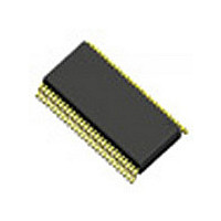
MK2069-03GI IDT, Integrated Device Technology Inc, MK2069-03GI Datasheet - Page 7

MK2069-03GI
Manufacturer Part Number
MK2069-03GI
Description
IC VCXO CLK TRANSLATOR 56-TSSOP
Manufacturer
IDT, Integrated Device Technology Inc
Type
Clock Synchronizerr
Datasheet
1.MK2069-03GITR.pdf
(20 pages)
Specifications of MK2069-03GI
Pll
Yes
Input
LVCMOS
Output
LVCMOS
Number Of Circuits
1
Ratio - Input:output
1:3
Differential - Input:output
No/No
Frequency - Max
160MHz
Divider/multiplier
Yes/No
Voltage - Supply
3.15 V ~ 3.45 V
Operating Temperature
-40°C ~ 85°C
Mounting Type
Surface Mount
Package / Case
56-TSSOP
Frequency-max
160MHz
Number Of Elements
2
Supply Current
30mA
Pll Input Freq (min)
1KHz
Pll Input Freq (max)
27MHz
Operating Supply Voltage (typ)
3.3V
Operating Temp Range
-40C to 85C
Package Type
TSSOP
Output Frequency Range
2.5 to 160MHz
Operating Supply Voltage (min)
3.15V
Operating Supply Voltage (max)
3.45V
Operating Temperature Classification
Industrial
Pin Count
56
Lead Free Status / RoHS Status
Contains lead / RoHS non-compliant
C
For higher damping factors (> 1), calculate the value of C
based on a C
of 1. This will minimize baseband peaking and loop
instability that can lead to output jitter.
C
charge pump correction pulses. A C
will result in increased output phase noise at the phase
detector frequency due to this. In extreme cases where
Graph of Charge Pump Current vs. Value of R
Charge Pump Current, Example Settings from
Notes on Setting Charge Pump Current
The recommended range for the charge pump current is 25
IDT™ / ICS™ VCXO-BASED CLOCK TRANSLATOR WITH HIGH MULTIPLICATION 7
P
P
MK2069-03
VCXO-BASED CLOCK TRANSLATOR WITH HIGH MULTIPLICATION
establishes a second pole in the VCXO PLL loop filter.
also dampens VCXO input voltage modulation by the
C
P
480 k
400 k
Above Graph
=
5 M
3 M
2 M
1 M
R
SET
C
----- -
20
S
S
value that would be used for a damping factor
Charge Pump Current
100E-6
10E-6
1E-3
100E+3
125 A
255 A
300 A
25 A
42 A
65 A
(I
CP
)
P
value that is too low
R
P
SET
SET
1E+6
, ohms
input jitter is high, charge pump current is high, and C
small, the VCXO input voltage can hit the supply or ground
rail resulting in non-linear loop response.
The best way to set the value of C
response software available from ICS (please refer to the
following section). C
just starts affecting the passband peak.
Loop Filter Response Software
Online tools to calculate loop filter response can be found at
www.idt.com/?app=calculators&source=support_menu.
to PCB or capacitor leakage, can become a problem. This
loop filter leakage can cause locking problems, output clock
cycle slips, or low frequency phase noise.
As can be seen in the loop bandwidth and damping factor
equations or by using the filter response software available
from ICS, increasing charge pump current (I
both bandwidth and damping factor.
(external resistor)
A to 300 A. Below 25 A, loop filter charge leakage, due
Recommended Range
of Operation
P
should be increased in value until it
VCXO AND SYNTHESIZER
10E+6
P
MK2069-03
is to use the filter
CP
) increases
REV J 030906
P
is too


