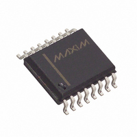
DS21610SN+ Maxim Integrated Products, DS21610SN+ Datasheet

DS21610SN+
Specifications of DS21610SN+
Related parts for DS21610SN+
DS21610SN+ Summary of contents
Page 1
... Frequency-Locked Output for all Operation Modes No External Components Required 16-Pin SO and 28-Pin PLCC Industrial Temperature Range: -40°C to +85°C ORDERING INFORMATION PART DS21610SN -40°C to +85°C DS21610SN+ -40°C to +85°C -40°C to +85°C DS21610QN DS21610QN+ -40°C to +85°C + Denotes a lead-free/RoHS-compliant device DS21610 TEMP RANGE ...
Page 2
PIN DESCRIPTION ........................................................................................................................ 3 1.1 C LXP610 .........................................................................................................................3 OMPATIBILITY WITH 2. FUNCTIONAL DESCRIPTION ....................................................................................................... 5 3. OUTPUT JITTER............................................................................................................................ 6 3 ...........................................................................................................................................6 ITTER RANSFER 4. OPERATING PARAMETERS......................................................................................................... 8 5. PACKAGE INFORMATION.......................................................................................................... 13 5.1 16-P SO (300 ) (56-G4009-001) ...
Page 3
PIN DESCRIPTION Table 1-A. Pin Description PIN NAME PLCC SYNCOUT 3–5, 7–9, 11, 12, 17– N.C. 19, 21, 23, 25 CLKOUT2 10 5 CLKIN 13 7 CLKOUT1 ...
Page 4
Figure 1-1. Block Diagram ANALOG CLKIN PLL DS21610 SEL SYNCIN P1 FREQUENCY P2 PLL SELECT P3 LOGIC P4 FEEDBACK OUTPUT CIRCUIT DIVIDER FRAME SYNC GENERATOR CLKOUT2 CLKOUT1 SYNCOUT FSP ...
Page 5
FUNCTIONAL DESCRIPTION A clock input at CLKIN is converted to various clocks available on CLKOUT1 and CLKOUT2. Additionally, an 8kHz clock locked to CLKIN and SYNCIN (if present) is always available at the SYNCOUT pin. The pulse width of ...
Page 6
OUTPUT JITTER Table 3-A shows the output jitter specifications for 2.048MHz (or 4.096MHz) to 1.544MHz conversions (SEL = 1) and 1.544MHz to 2.048MHz (or 4.096MHz) conversions (SEL = 0). Table 3-A. Output Jitter Specifications, CLKOUT1 = 1.544MHz FREQUENCY BAND ...
Page 7
Figure 3-2. Nominal Jitter Transfer (2.048MHz CLKIN to 1.544MHz CLKOUT1) 2 1.8 1.6 1.4 1.2 1 0.8 0.6 0.4 0 NOTE: THE TYPICAL PEAK JITTER GAIN OF THE DS2161 IS ABOUT 1.4 FOR CONVERSION FROM T1 TO ...
Page 8
OPERATING PARAMETERS ABSOLUTE MAXIMUM RATINGS Voltage Range on Any Pin Relative to Ground…………………………………………………………..-1.0V to +6.0V Operating Temperature Range for DS21610SN………………………………………………………...-40°C to +85°C Storage Temperature Range……………………………………………………………………………..-55°C to +125°C Soldering Temperature………………………………………………………See IPC/JEDEC J-STD-020 Specification Stresses beyond those listed under “Absolute Maximum ...
Page 9
AC TIMING (Figure 4-1, Figure 4-2, Figure 4-3, PARAMETER Capture Range on CLKIN Lock Range on CLKIN CLKIN Duty Cycle SYNCIN Setup to CLKIN Rising SYNCIN Hold After CLKIN Rising SYNCIN Pulse Width CLKOUT1 Delay from CLKIN Rising CLKOUT1 Duty ...
Page 10
Figure 4-1. SYNCIN/CLKIN to CLKOUT1/SYNCOUT and CLKOUT2 CLKIN SINCIN CLKOUT1 CLKOUT1 SYNCOUT CLKOUT2 CLKOUT1 ...
Page 11
Figure 4-2. Output Frame-Sync Alignment When CLKOIT2 = 2 x CLKOUT1 CLKOUT1 (4.096MHz) CLKOUT2 (8.192MHz) SYNCOUT CLKOUT1 (3.088MHz) CLKOUT2 (6.176MHz) SYNCOUT Figure 4-3. Output Frame-Sync Alignment When CLKOUT2 = 3 x CLKOUT1 CLKOUT1 (2.56MHz or 2.048MHz) CLKOUT2 (7.680MHz or 6.144MHz) ...
Page 12
Figure 4-4. Output Frame-Sync Alignment When CLKOIT2 = 4 x CLKOUT1 CLKOUT1 (1.544MHz or 2.048MHz) CLKOUT2 (6.176MHz or 8.192MHz) SYNCOUT (short) SYNCOUT (long) Figure 4-5. Output Frame-Sync Alignment When CLKOUT2 = 5 x CLKOUT1 CLKOUT1 (1.544MHz) CLKOUT2 (7.720MHz) SYNCOUT 12 ...
Page 13
PACKAGE INFORMATION (The package drawing(s) in this data sheet may not reflect the most current specifications. The package number provided for each package is a link to the latest package outline information.) 5.1 16-Pin SO (300 mils) (56-G4009-001) 13 ...
Page 14
PLCC (56-G4001-001 ...
Page 15
... No circuit patent licenses are implied. Maxim/Dallas Semiconductor reserves the right to change the circuitry and specifications without notice at any time The Maxim logo is a registered trademark of Maxim Integrated Products, Inc. The Dallas logo is a registered trademark of Dallas Semiconductor Corporation. DESCRIPTION © 2006 Maxim Integrated Products • Printed USA ...


