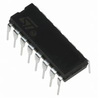
HCF4046BEY STMicroelectronics, HCF4046BEY Datasheet

HCF4046BEY
Specifications of HCF4046BEY
Available stocks
Related parts for HCF4046BEY
HCF4046BEY Summary of contents
Page 1
... A comparators having a common signal-input amplifier and a common comparator input. A 5.2V zener diode is provided for supply regulation if necessary. HCF4046B DIP SOP TUBE T & R HCF4046BEY HCF4046BM1 HCF4046M013TR in Metal Oxide Semiconductor (VCO) and two different phase 1/12 ...
Page 2
HCF4046B VCO Section The VCO requires one external capacitor C1 and one or two external resistors ( and R2). Resistor R1 and capacitor C1 determine the frequency range of the VCO and resistor R2 enables the VCO to ...
Page 3
ON for a time corresponding to the phase Subsequently, the capacitor voltage of the low-pass filter connected to this phase comparator is adjusted until the signal and comparator inputs are equal in both phase and ...
Page 4
HCF4046B Figure 3 : Typical Waveforms for CMOS Phase-locked Loop Employing Phase Comparator II In Locked Condition INPUT EQUIVALENT CIRCUIT 4/12 PIN DESCRIPTION PIN No SYMBOL NAME AND FUNCTION 1 PHASE PULSES Phase Comparator Pulse Output 2 PHASE COMP I ...
Page 5
FUNCTIONAL DIAGRAM ABSOLUTE MAXIMUM RATINGS Symbol V Supply Voltage Input Voltage Input Current I P Power Dissipation per Package D Power Dissipation per Output Transistor T Operating Temperature op T Storage Temperature stg Absolute ...
Page 6
HCF4046B DC SPECIFICATIONS Symbol Parameter V (V) VCO SECTION V High Level Output 0/5 OH Voltage 0/10 0/15 V Low Level Output 5/0 OL Voltage 10/0 15/0 I Output Drive 0/5 OH Current 0/5 0/10 0/15 I Output Sink 0/5 ...
Page 7
ELECTRICAL CHARACTERISTICS (T Symbol Parameter VCO SECTION P Operating Power D Dissipation f Maximum MAX frequency Center Frequency (f ) and frequency O Range max min Linearity Temperature Frequency Stability (no frequency offset min ...
Page 8
HCF4046B Symbol Parameter PHASE COMPARATOR SECTION R14 Pin 14 (signal in) Input Resistance AC Coupled Signal Input Sensivity (*) (peak to peak) t Propagation Delay PLH Time High to Low Level Pins Propagation Delay PLH Time ...
Page 9
DESIGN INFORMATION This information is a guide for approximating the value of external components in a Phase-Locked-Loop system. The selected external components must be within the following ranges USING ...
Page 10
HCF4046B DIM. MIN. a1 0. 10/12 Plastic DIP-16 (0.25) MECHANICAL DATA mm. TYP MAX. 1.65 0.5 0.25 20 8.5 2.54 17.78 7.1 5.1 3.3 1.27 inch MIN. TYP. ...
Page 11
SO-16 MECHANICAL DATA mm. DIM. MIN 0 0. 9 3.8 G 4 TYP MAX. MIN. 1.75 0.2 0.003 1.65 0.46 0.013 0.25 ...
Page 12
... No license is granted by implication or otherwise under any patent or patent rights of STMicroelectronics. Specifications mentioned in this publication are subject to change without notice. This publication supersedes and replaces all information previously supplied ...


