LTC6900CS5#TRMPBF Linear Technology, LTC6900CS5#TRMPBF Datasheet
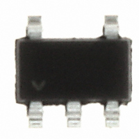
IC OSC PREC 1KHZ-20MHZ TSOT23-5

LTC6900CS5#TRMPBF

Manufacturer Part Number
LTC6900CS5#TRMPBF
Description
IC OSC PREC 1KHZ-20MHZ TSOT23-5
Manufacturer
Linear Technology
Type
Oscillator, Siliconr
Datasheet

Specifications of LTC6900CS5#TRMPBF

Frequency
20MHz
Voltage - Supply
2.7 V ~ 5.5 V
Current - Supply
920µA
Operating Temperature
-40°C ~ 85°C
Package / Case
TSOT-23-5, TSOT-5, TSOP-5
Lead Free Status / RoHS Status
Lead free / RoHS Compliant
Count
-
Other names
LTC6900CS5#TRMPBFTR

Available stocks

Company
Part Number
Manufacturer
Quantity
Price
Company:
Part Number:
LTC6900CS5#TRMPBFLTC6900CS5
Manufacturer:
LT
Quantity:
10 000
Company:
Part Number:
LTC6900CS5#TRMPBFLTC6900CS5
Manufacturer:
LTNEAR
Quantity:
20 000
Company:
Part Number:
LTC6900CS5#TRMPBFLTC6900CS5#TRP
Manufacturer:
LT
Quantity:
20 000
Company:
Part Number:
LTC6900CS5#TRMPBFLTC6900CS5#TRPBF
Manufacturer:
LT
Quantity:
3 928
Company:
Part Number:
LTC6900CS5#TRMPBFLTC6900CS5#TRPBF
Manufacturer:
LT
Quantity:
20 000
APPLICATIONS
TYPICAL APPLICATION
FEATURES
n
n
n
n
n
n
n
n
n
n
n
n
n
n
n
n
n
n
n
n
n
n
10k ≤ R
One External Resistor Sets the Frequency
1kHz to 20MHz Frequency Range
500μA Typical Supply Current, V
Frequency Error ≤1.5% Max, 5kHz to 10MHz
(T
Frequency Error ≤ 2% Max, 5kHz to 10MHz
(T
±40ppm/°C Temperature Stability
0.04%/V Supply Stability
50% ±1% Duty Cycle 1kHz to 2MHz
50% ± 5% Duty Cycle 2MHz to 10MHz
Fast Start-Up Time: 50μs to 1.5ms
100Ω CMOS Output Driver
Operates from a Single 2.7V to 5.5V Supply
Low Profi le (1mm) ThinSOT™ Package
Portable and Battery-Powered Equipment
PDAs
Cell Phones
Low Cost Precision Oscillator
Charge Pump Driver
Switching Power Supply Clock Reference
Clocking Switched Capacitor Filters
Fixed Crystal Oscillator Replacement
Ceramic Oscillator Replacement
A
A
SET
= 25°C)
= 0°C to 70°C)
≤ 2M
5V
f
OSC
0.1μF
= 10MHz •
Clock Generator
(
1
2
3
N • R
20k
V
GND
SET
+
LTC6900
SET
)
6900 TA01a
OUT
DIV
5
4
1kHz ≤ f
S
N = 1
= 3V, 3MHz
5V, N = 100
OSC
≤ 20MHz
OPEN, N = 10
Resistor Set SOT-23 Oscillator
DESCRIPTION
L, LT, LTC, LTM, Linear Technology and the Linear logo are registered trademarks of Linear
Technology Corporation. ThinSOT is a trademark of Linear Technology Corporation.
The LTC
easy to use and occupies very little PC board space. The
oscillator frequency is programmed by a single external
resistor (R
accuracy operation (≤1.5% frequency error) without the
need for external trim components.
The LTC6900 operates with a single 2.7V to 5.5V power
supply and provides a rail-to-rail, 50% duty cycle square
wave output. The CMOS output driver ensures fast rise/fall
times and rail-to-rail switching. The frequency-setting
resistor can vary from 10kΩ to 2MΩ to select a master
oscillator frequency between 100kHz and 20MHz (5V
supply). The three-state DIV input determines whether the
master clock is divided by 1, 10 or 100 before driving the
output, providing three frequency ranges spanning 1kHz
to 20MHz (5V supply). The LTC6900 features a proprietary
feedback loop that linearizes the relationship between R
and frequency, eliminating the need for tables to calculate
frequency. The oscillator can be easily programmed using
the simple formula outlined below:
All other trademarks are the property of their respective owners.
f
Low Power, 1kHz to 20MHz
OSC
= 10MHz •
®
10000
1000
6900 is a precision, low power oscillator that is
100
10
SET
1
1k
R
). The LTC6900 has been designed for high
SET
DESIRED OUTPUT FREQUENCY (Hz)
⎝ ⎜
÷100
10k
vs Desired Output Frequency
N•R
20k
SET
÷10
100k
⎠ ⎟
, N =
÷1
1M
100,
10,
1,
10M
6900 TA01b
LTC6900
DIV Pin = V
DIV Pin = Open
DIV Pin = GND
100M
+
6900fa
1
SET

Related parts for LTC6900CS5#TRMPBF

LTC6900CS5#TRMPBF Summary of contents

Page 1

... OSC L, LT, LTC, LTM, Linear Technology and the Linear logo are registered trademarks of Linear Technology Corporation. ThinSOT is a trademark of Linear Technology Corporation. All other trademarks are the property of their respective owners. 10000 1kHz ≤ f ≤ ...

Page 2

LTC6900 ABSOLUTE MAXIMUM RATINGS (Note 1) + Supply Voltage ( GND .........................– 0. DIV to GND .................................... –0. SET to GND ....................................– 0. Operating Temperature Range (Note 8) LTC6900C ............................................– 40°C to ...

Page 3

ELECTRICAL CHARACTERISTICS temperature range, otherwise specifi cations are at T All voltages are with respect to GND. SYMBOL PARAMETER + V Operating Supply Range I Power Supply Current S V High Level DIV Input Voltage IH V Low Level DIV ...

Page 4

LTC6900 TYPICAL PERFORMANCE CHARACTERISTICS Frequency Variation vs R SET 25° GUARANTEED LIMITS APPLY OVER 20kΩ ≤ R ≤ 400kΩ SET 2 TYPICAL HIGH 1 0 –1 TYPICAL LOW –2 –3 –4 1k 10k 100k 1M ...

Page 5

PIN FUNCTIONS + V (Pin 1): Voltage Supply (2.7V ≤ V must be kept free from noise and ripple. It should be by- passed directly to a ground plane with a 0.1μF capacitor. GND (Pin 2): Ground. Should be tied ...

Page 6

LTC6900 OPERATION As shown in the Block Diagram, the LTC6900’s master os- cillator is controlled by the ratio of the voltage between the + V and SET pins and the current (I RES pin. The voltage on the SET pin ...

Page 7

APPLICATIONS INFORMATION SELECTING THE DIVIDER SETTING AND RESISTOR The LTC6900’s master oscillator has a frequency range spanning 0.1MHz to 20MHz. However, accuracy may suffer if the master oscillator is operated at greater than 10MHz with a supply voltage lower than ...

Page 8

LTC6900 APPLICATIONS INFORMATION POWER SUPPLY REJECTION Low Frequency Supply Rejection (Voltage Coeffi cient) Figure 5 shows the output frequency sensitivity to power supply voltage at several different temperatures. The LTC6900 has a guaranteed voltage coeffi cient of 0.1%/V but, as ...

Page 9

APPLICATIONS INFORMATION OUT LTC6900 SET1 GND ÷100 R SET2 3 4 ÷10 SET DIV ÷1 6900 F07 Figure 7 A Ground Referenced Voltage Controlled Oscillator The LTC6900 output ...

Page 10

LTC6900 APPLICATIONS INFORMATION Once known, calculate R IN SET 10MHz 20k = R • • SET N f OSC(MAX) ⎡ ⎛ − ⎢ ⎝ ⎜ IN(MAX) RES R ...

Page 11

... JEDEC PACKAGE REFERENCE IS MO-193 Information furnished by Linear Technology Corporation is believed to be accurate and reliable. However, no responsibility is assumed for its use. Linear Technology Corporation makes no representa- tion that the interconnection of its circuits as described herein will not infringe on existing patent rights. Maximum modulation bandwidth is the lesser of 25kHz or ...

Page 12

... YSI 44011 800 765-4974 T Output Frequency vs Temperature 1400 MAX TYP 1200 MIN 1000 800 600 400 200 0 –20 – TEMPERATURE (°C) 6900 TA03 COMMENTS Identical Pinout, Higher Frequency Operation www.linear.com ● 20k • 0709 REV A • PRINTED IN USA © LINEAR TECHNOLOGY CORPORATION 2002 6900fa ...

Related keywords