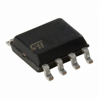
TS555IDT STMicroelectronics, TS555IDT Datasheet - Page 13

TS555IDT
Manufacturer Part Number
TS555IDT
Description
IC TIMER LP SINGLE CMOS 8 SOIC
Manufacturer
STMicroelectronics
Type
555 Type, Timer/Oscillator (Single)r
Datasheet
1.TS555CDT.pdf
(20 pages)
Specifications of TS555IDT
Frequency
2.7MHz
Voltage - Supply
2 V ~ 16 V
Current - Supply
65µA
Operating Temperature
-40°C ~ 125°C
Package / Case
8-SOIC (3.9mm Width)
Number Of Internal Timers
1
Supply Voltage (max)
2 V to 16 V
Supply Voltage (min)
2 V
Maximum Power Dissipation
715 mW
Maximum Operating Temperature
125 C
Minimum Operating Temperature
- 40 C
Mounting Style
SMD/SMT
Propagation Delay (max)
100 ns (Typ) @ 3 V to 5 V
Lead Free Status / RoHS Status
Lead free / RoHS Compliant
Count
-
Lead Free Status / Rohs Status
Lead free / RoHS Compliant
Other names
497-2298-2
Available stocks
Company
Part Number
Manufacturer
Quantity
Price
Company:
Part Number:
TS555IDT
Manufacturer:
ST
Quantity:
50 000
Part Number:
TS555IDT
Manufacturer:
ST
Quantity:
20 000
Part Number:
TS555IDTTR
Manufacturer:
ST
Quantity:
20 000
TS555
4.2
Astable operation
When the circuit is connected as shown in
and runs as a multi-vibrator. The external capacitor charges through R
discharges through R
these two resistors.
In the astable mode of operation, C charges and discharges between 1/3 V
As in the triggered mode, the charge and discharge times, and therefore frequency, are
independent of the supply voltage.
Figure 6.
Figure 7
The charge time (output HIGH) is given by:
The discharge time (output LOW) by:
Thus the total period T is given by:
The frequency of oscillation is then:
The duty cycle is given by:
Figure 7.
shows actual waveforms generated in this mode of operation.
t1 = 0.693 (R
t2 = 0.693 x R
T = t1 + t2 = 0.693 (R
Application schematic
Timing diagram
B
A
only. Therefore, the duty cycle may be precisely set by the ratio of
B
+ R
D =
f =
x C
B
) C
1
-- - =
T
Voltage
0.01 F
---------------------------
RA
Control
A
V
μ
RB
CC
------------------------------------- -
(RA
Out
+ 2R
+
R = R = 4.8 k , C = 0.1 F , R = 1.0k
2RB
A
t = 0.5 ms / div
OUTPUT VOLTAGE = 5.0V/div
CAPACITOR VOLTAGE = 1.0V/div
+
1.44
B
B
2RB )C
) C
5
Reset
3
Figure 6
1
Ω
4
TS555
μ
8
2
(pins 2 and 6 connected) it triggers itself
L
7
6
Ω
R
R
C
B
A
Application information
A
and R
CC
B
and 2/3 V
and
13/20
CC
.


