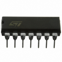
TS556IN STMicroelectronics, TS556IN Datasheet - Page 12

TS556IN
Manufacturer Part Number
TS556IN
Description
IC TIMER LP DUAL CMOS 14 DIP
Manufacturer
STMicroelectronics
Type
555 Type, Timer/Oscillator (Dual)r
Datasheet
1.TS556IDT.pdf
(19 pages)
Specifications of TS556IN
Frequency
2.7MHz
Voltage - Supply
2 V ~ 16 V
Current - Supply
130µA
Operating Temperature
-40°C ~ 125°C
Package / Case
14-DIP (0.300", 7.62mm)
Number Of Internal Timers
2
Supply Voltage (max)
16 V
Supply Voltage (min)
2 V
Maximum Power Dissipation
1560 mW
Maximum Operating Temperature
+ 125 C
Minimum Operating Temperature
- 40 C
Mounting Style
Through Hole
Propagation Delay (max)
100 ns (Typ) @ 3 V to 5 V
Lead Free Status / RoHS Status
Lead free / RoHS Compliant
Count
-
Lead Free Status / Rohs Status
Lead free / RoHS Compliant
Other names
497-2301-5
Available stocks
Company
Part Number
Manufacturer
Quantity
Price
Company:
Part Number:
TS556IN
Manufacturer:
FUJI
Quantity:
9 200
Part Number:
TS556IN
Manufacturer:
ST
Quantity:
20 000
Application information
4
4.1
12/19
Application information
Monostable operation
In the monostable mode, the timer operates like a one-shot generator. Referring to figure 2,
the external capacitor is initially held discharged by a transistor inside the timer, as shown in
Figure
Figure 4.
The circuit triggers on a negative-going input signal when the level reaches 1/3 V
triggered, the circuit remains in this state until the set time has elapsed, even if it is triggered
again during this interval. The duration of the output HIGH state is given by t = 1.1 R x C.
It can be noticed that since the charge rate and the threshold level of the comparator are
both directly proportional to the supply voltage, the timing interval is independent of the
supply. Applying a negative pulse simultaneously to the Reset terminal (pin 4) and the
Trigger terminal (pin 2) during the timing cycle discharges the external capacitor and causes
the cycle to start over. The timing cycle now starts on the positive edge of the reset pulse.
While the reset pulse is applied, the output is driven to the LOW state.
When a negative trigger pulse is applied to pin 2, the flip-flop is set, releasing the short
circuit across the external capacitor and driving the output HIGH. The voltage across the
capacitor increases exponentially with the time constant τ = R x C.
When the voltage across the capacitor equals 2/3 V
which then discharges the capacitor rapidly and drives the output to its LOW state.
Figure 5
When Reset is not used, it should be tied high to avoid any possible or false triggering.
Figure 5.
4.
shows the actual waveforms generated in this mode of operation.
Application schematic
Timing diagram
Trigger
V
Out
CC
R = 9.1k , C = 0.01 F , R = 1.0k
t = 0.1 ms / div
OUTPUT VOLTAGE = 5.0V/div
INPUT = 2.0V/div
CAPACITOR VOLTAGE = 2.0V/div
Reset
Ω
TS556
1/2
μ
L
CC
, the comparator resets the flip-flop
Ω
Control Voltage
R
C
0.01 F
μ
CC
. Once
TS556


