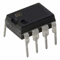
SE555N STMicroelectronics, SE555N Datasheet

SE555N
Specifications of SE555N
SE555N
Available stocks
Related parts for SE555N
SE555N Summary of contents
Page 1
Features ■ Low turn-off time ■ Maximum operating frequency greater than 500 kHz ■ Timing from microseconds to hours ■ Operates in both astable and monostable modes ■ Output can source or sink up to 200 mA ■ Adjustable duty ...
Page 2
Schematic diagrams 1 Schematic diagrams Figure 1. Block diagram Figure 2. Schematic diagram 2/ 5kΩ COMP THRESHOLD R CONTROL VOLTAGE FLIP-FLOP Q 5kΩ COMP TRIGGER S INHIBIT/ RESET 5kΩ S RESET S - 8086 NE555 - SA555 ...
Page 3
NE555 - SA555 - SE555 2 Absolute maximum ratings and operating conditions Table 1. Absolute maximum ratings Symbol V Supply voltage CC I Output current (sink & source) OUT Thermal resistance junction to ambient R thja Thermal resistance junction to ...
Page 4
Electrical characteristics 3 Electrical characteristics Table +25° amb Symbol Parameter = ∝ ) Supply current (R L Low state +15V CC High state V = +5V CC ...
Page 5
NE555 - SA555 - SE555 Table +25° amb Symbol Parameter Discharge pin leakage current I dis(off) (output high 10V dis Discharge pin saturation voltage (4) (output low) V dis(sat +15V, I ...
Page 6
Electrical characteristics Figure 3. Minimum pulse width required for triggering Figure 5. Delay time versus temperature Figure 7. Low output voltage versus output sink current 6/20 NE555 - SA555 - SE555 Figure 4. Supply current versus supply voltage Figure 6. ...
Page 7
NE555 - SA555 - SE555 Figure 9. High output voltage drop versus output Figure 11. Propagation delay versus voltage level of trigger value Electrical characteristics Figure 10. Delay time versus supply voltage 7/20 ...
Page 8
Application information 4 Application information 4.1 Monostable operation In the monostable mode, the timer generates a single pulse. As shown in external capacitor is initially held discharged by a transistor inside the timer. Figure 12. Typical schematics in monostable operation ...
Page 9
NE555 - SA555 - SE555 Figure 13. Waveforms in monostable operation Figure 14. Pulse duration versus R1C1 4.2 Astable operation When the circuit is connected as shown in itself and free runs as a multi-vibrator. The external capacitor charges through ...
Page 10
Application information Figure 15. Typical schematics in astable operation V CC 0.01 Figure 16 shows the actual waveforms generated in this mode of operation. The charge time (output HIGH) is given by 0.693 (R and the discharge time ...
Page 11
NE555 - SA555 - SE555 Figure 16. Waveforms in astable operation Figure 17. Free running frequency versus 0 div OUTPUT VOLTAGE = 5.0V/div CAPACITOR VOLTAGE = 1.0V/div Ω 4.8k , C1= ...
Page 12
Application information 4.3 Pulse width modulator When the timer is connected in the monostable mode and triggered with a continuous pulse train, the output pulse width can be modulated by a signal applied to pin 5. the circuit. Figure 18. ...
Page 13
NE555 - SA555 - SE555 Figure 20 shows the waveforms generator by the linear ramp. The time interval is given by: Figure 20. Linear ramp 4.5 50% duty cycle oscillator For a 50% duty cycle, the resistors R period for ...
Page 14
Application information Figure 21. 50% duty cycle oscillator Out Note that this circuit will not oscillate if R and R cannot bring pin 2 down to 1 4.6 Additional information Adequate power supply bypassing is necessary to protect ...
Page 15
... JEDEC Standard JESD97. The maximum ratings related to soldering conditions are also marked on the inner box label. ECOPACK is an STMicroelectronics trademark. ECOPACK specifications are available at: www.st.com. Package information ...
Page 16
Package information 5.1 DIP8 package information Figure 22. DIP8 package mechanical drawing Table 4. DIP8 package mechanical data Ref 16/20 Dimensions Millimeters Min. Typ. Max. 5.33 0.38 ...
Page 17
NE555 - SA555 - SE555 5.2 SO-8 package information Figure 23. SO-8 package mechanical drawing Table 5. SO-8 package mechanical data Ref ccc Dimensions Millimeters Min. Typ. ...
Page 18
... Package DIP8 0°C, +70°C SO-8 DIP8 -40°C, +105°C SO-8 DIP8 -55°C, + 125°C SO-8 NE555 - SA555 - SE555 Packing Marking Tube NE555N Tube or tape & reel NE555 Tube SA555N Tube or tape & reel SA555 Tube SE555N Tube or tape & reel SE555 ...
Page 19
NE555 - SA555 - SE555 7 Revision history Table 7. Document revision history Date 01-Jun-2003 2004-2006 15-Mar-2007 06-Nov-2008 Revision 1 Initial release. 2-3 Internal revisions Expanded order code table. 4 Template update. Added I value in OUT Table 2: Operating ...
Page 20
... Information in this document is provided solely in connection with ST products. STMicroelectronics NV and its subsidiaries (“ST”) reserve the right to make changes, corrections, modifications or improvements, to this document, and the products and services described herein at any time, without notice. All ST products are sold pursuant to ST’s terms and conditions of sale. ...


