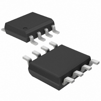
DS1077Z-100+ Maxim Integrated Products, DS1077Z-100+ Datasheet

DS1077Z-100+
Specifications of DS1077Z-100+
Related parts for DS1077Z-100+
DS1077Z-100+ Summary of contents
Page 1
... CC GND 4 150mil SO 118mil µSOP Package PIN DESCRIPTION OUT1 OUT0 V CC GND CTRL1 CTRL0 SDA SCL ORDERING INFORMATION Note: XXX denotes frequency option DS1077Z-XXX 8.1kHz DS1077U-XXX DS1077 8 SCL 7 SDA 6 CTRL1 5 CTRL0 - Main Oscillator Output - Reference Output - Power Supply Voltage - Ground - Control Pin for OUT1 ...
Page 2
BLOCK DIAGRAM 1077 Figure1 INTERNAL OSCILLATOR MCLK DIV1 0M1 0M0 1M1 1M0 EN0 SEL0 PDN0 PDN1 CONTROL REGISTERS 2-WIRE INTERFACE SDA SCL SEL0 EN0 PDN0 MUX P0 PRESCALER (M DIVIDER) 0M1 0M0 P1 PRESCALER (M DIVIDER) Power-Down 1M1 1M0 PDN1 ...
Page 3
OVERVIEW A block diagram of the DS1077 is shown in Figure 1. The DS1077 consists of four major components: 1) Internal Master Oscillator, 2) Prescalers, 3) Programmable Divider, and 4) Control Registers. The internal oscillator is factory-trimmed to provide a ...
Page 4
DEVICE MODE USING OUT0 Table 1 EN0 SEL0 PDN0 (BIT) (BIT) (BIT *This mode is for applications where OUT0 is not used, ...
Page 5
SHUTDOWN CONTROL WITH PDN0 AND PDN1 Table 3 PDN0 PDN1 (BIT) (BIT *CTRL0 performs a power-down if SEL0 and EN0 are both 0 (see Table 1). REGISTER FUNCTIONS The user programmable registers ...
Page 6
EN0 (bit EN0 = 1 and PDN0 = 0 the CTRL0 pin functions as an Output Enable for OUT0, the frequency of the output being determined by the SEL0 bit PDN0 = 1, the EN0 bit ...
Page 7
DIV WORD MSB first data byte N These ten bits determine the value of the programmable divider (N). The range of divisor values is from 2 to 1025, and is equal to the programmed value ...
Page 8
SERIAL DATA BUS The DS1077 supports a bidirectional 2-wire bus and data transmission protocol. A device that sends data onto the bus is defined as a transmitter, and a device receiving data as a receiver. The device that controls ...
Page 9
DATA TRANSFER ON 2-WIRE SERIAL BUS Figure 2 SDA MSB SCL 1 START CONDITION Figure 2 details how data transfer is accomplished on the 2-wire bus. Depending upon the state of the R/ bit, two types of data transfer are ...
Page 10
SLAVE ADDRESS A control byte is the first byte received following the START condition from the master device. The control byte consists of a 4-bit control code; for the DS1077, this is set as 1011 binary for read and write ...
Page 11
SERIAL COMMUNICATION WITH DS1077 Figure 3 Send a “Standalone” Command SCL SDA Start Address Byte Write MSB of a Two-Byte Register SCL SDA ...
Page 12
SERIAL COMMUNICATION WITH DS1077 Figure 3 (continued) Read Single Byte Register or MSB from a Two-Byte Register SCL SDA Start Control Byte DS1077 ACK Read from a Two-Byte ...
Page 13
COMMAND SET Data and control information is read from and written to the DS1077 in the format shown in Figure 3. To write to the DS1077, the master will issue the slave address of the DS1077 and the R/ After ...
Page 14
ABSOLUTE MAXIMUM RATINGS Voltage on Any Pin Relative to Ground Operating Temperature Range Programming Temperature Range Storage Temperature Range Soldering Temperature DC ELECTRICAL CHARACTERISTICS PARAMETER SYMBOL Supply Voltage High-Level Output Voltage (OUT1,OUT0) Low-Level Output Voltage (OUT1,OUT0) High-Level Input Voltage (CTRL1, ...
Page 15
AC ELECTRICAL CHARACTERISTICS PARAMETER Output Frequency Tolerance Over Temperature Output Frequency Tolerance Over Voltage Combined Freq. Variation Output Frequency Min Output Frequency Max Power-Up Time Enable OUT1 from PDN Enable OUT0 from PDN OUT1 Hi-Z from PDN OUT0 Hi-Z from ...
Page 16
AC ELECTRICAL CHARACTERISTICS: 2-WIRE INTERFACE PARAMETER SYMBOL SCL Clock Frequency Bus Free Time Between a STOP and START Condition Hold Time (Repeated) START Condition LOW Period of SCL HIGH Period of SCL Set-Up Time for a Repeated START Data Hold ...
Page 17
... TIMING DIAGRAM SDA t BUF t t LOW R SCL t HD:STA t HD:DAT STOP START ORDERING INFORMATION DS1077 Example: DS1077Z-100 = 1000ns + 250ns = 1250ns before the SCL line is released HIGH SU:STA SU:DAT REPEATED START 133 = 133.333MHz 125 = 125.000MHz 120 = 120.000MHz 100 = 100.000MHz > ...
Page 18
TYPICAL OPERATING CHARACTERISTICS (V = 5.0V +25°C, unless otherwise specified) CC 45.00 40.00 35.00 30.00 25.00 20.00 15.00 10.00 5.00 0.00 4 SUPPLY CURRENT vs. VOLTAGE DS1077-133 DS1077-100 DS1077-66 ...
Page 19
TYPICAL OPERATING CHARACTERISTICS (continued 5.0V +25°C, unless otherwise specified SUPPLY CURRENT vs. TEMPERATURE SUPPLY CURRENT vs. DIVISOR (N) DS1077-133 ...
Page 20
TYPICAL OPERATING CHARACTERISTICS (continued 5.0V +25°C, unless otherwise specified) CC 1.5 0.5 -0.5 -1 -1.5 -2 2.00 1.50 1.00 0.50 0.00 -0.50 -1.00 -1.50 -2.00 TEMPCO MUX=3040h DIV=0000h ...
Page 21
TYPICAL OPERATING CHARACTERISTICS (continued 5.0V +25°C, unless otherwise specified 3.5 3 2.5 2 1.5 1 0.5 0 SHUTDOWN CURRENT vs. TEMPERATURE DS1077- EMPERAT URE ( ...


