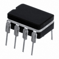
LM555J National Semiconductor, LM555J Datasheet - Page 8

LM555J
Manufacturer Part Number
LM555J
Description
IC TIMER HIGH TEMPERATURE 8-CDIP
Manufacturer
National Semiconductor
Type
555 Type, Timer/Oscillator (Single)r
Datasheet
1.LM555J.pdf
(12 pages)
Specifications of LM555J
Voltage - Supply
4.5 V ~ 16 V
Current - Supply
10mA
Operating Temperature
-55°C ~ 125°C
Package / Case
8-CDIP (0.300", 7.62mm)
Frequency
100kHz
Lead Free Status / RoHS Status
Contains lead / RoHS non-compliant
Count
-
Lead Free Status / Rohs Status
Not Compliant
Other names
*LM555J
Available stocks
Company
Part Number
Manufacturer
Quantity
Price
Part Number:
LM555J
Manufacturer:
NS/国半
Quantity:
20 000
Company:
Part Number:
LM555J/883Q
Manufacturer:
Fujitsu
Quantity:
1
Part Number:
LM555J/883Q
Manufacturer:
NS/国半
Quantity:
20 000
www.national.com
Applications Information
Figure 13 shows waveforms generated by the linear ramp.
The time interval is given by:
V
TIME = 20 µs/DIV. Middle Trace: Output 5V/Div.
R
R
R
C = 0.01 µF
50% DUTY CYCLE OSCILLATOR
For a 50% duty cycle, the resistors R
nected as in Figure 14 . The time period for the output high is
the same as previous, t
is t
CC
1
2
E
= 47 k
= 100 k
= 2.7 k
2
= 5V
=
Bottom Trace: Capacitor Voltage 1V/Div.
FIGURE 13. Linear Ramp
Top Trace: Input 3V/Div.
1
V
= 0.693 R
BE
0.6V
A
C. For the output low it
A
and R
(Continued)
B
may be con-
DS007851-17
8
Thus the frequency of oscillation is
Note that this circuit will not oscillate if R
R
down to 1/3 V
ADDITIONAL INFORMATION
Adequate power supply bypassing is necessary to protect
associated circuitry. Minimum recommended is 0.1 µF in par-
allel with 1 µF electrolytic.
Lower comparator storage time can be as long as 10 µs
when pin 2 is driven fully to ground for triggering. This limits
the monostable pulse width to 10 µs minimum.
Delay time reset to output is 0.47 µs typical. Minimum reset
pulse width must be 0.3 µs, typical.
Pin 7 current switches within 30 ns of the output (pin 3) volt-
age.
A
because the junction of R
FIGURE 14. 50% Duty Cycle Oscillator
CC
and trigger the lower comparator.
A
and R
B
B
cannot bring pin 2
is greater than 1/2
DS007851-18


