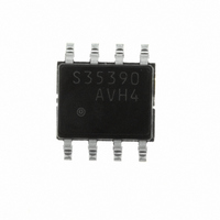
S-35390A-J8T1G Seiko Instruments, S-35390A-J8T1G Datasheet - Page 3

S-35390A-J8T1G
Manufacturer Part Number
S-35390A-J8T1G
Description
IC RTC I2C 2-WIRE 8-SOP
Manufacturer
Seiko Instruments
Type
Clock/Calendarr
Datasheet
1.S-35390A-J8T1G.pdf
(56 pages)
Specifications of S-35390A-J8T1G
Time Format
HH:MM:SS (12/24 hr)
Date Format
YY-MM-DD-dd
Interface
I²C, 2-Wire Serial
Voltage - Supply
1.3 V ~ 5.5 V
Operating Temperature
-40°C ~ 85°C
Mounting Type
Surface Mount
Package / Case
8-SOP
Lead Free Status / RoHS Status
Lead free / RoHS Compliant
Memory Size
-
Other names
728-1006-2
Available stocks
Company
Part Number
Manufacturer
Quantity
Price
Part Number:
S-35390A-J8T1G
Manufacturer:
SEIKO/精工
Quantity:
20 000
Rev.3.0
Pin Function
Equivalent Circuits of I/O Pin
•
•
•
•
•
•
•
SDA
This pin is to data input/output for I
SDA (I/O for serial data) pin
from the SCL pin. This pin has CMOS input and Nch open drain output. Generally in use, pull up this pin to the VDD
potential via a resistor, and connect it to any other device having open drain or open collector output with wired-OR
connection.
SCL (input for serial clock) pin
This pin is to input a clock pulse for I
pulse.
XIN, XOUT (crystal oscillator connect) pin
Connect a crystal oscillator between XIN and XOUT.
This pin outputs a signal of interrupt, or a clock pulse. By using the status register 2, users can select either of; alarm 1
interrupt, output of user-set frequency, per-minute edge interrupt, minute-periodical interrupt 1, minute-periodical
interrupt 2, or 32.768 kHz output. This pin has Nch open drain output.
This pin outputs a signal of interrupt, or a clock pulse. By using the status register 2, users can select either of; alarm 2
interrupt, output of user-set frequency, per-minute edge interrupt or minute-periodical interrupt 1. This pin has Nch
open drain output.
VDD (positive power supply) pin
Connect this VDD pin with a positive power supply. Regarding the values of voltage to be applied, refer to “
Recommended Operation Conditions”.
VSS pin
Connect this VSS pin to GND.
INT
INT
2
1
_00
(output for interrupt signal 1) pin
(output for interrupt signal 2) pin
Figure 4 SDA Pin
2
C-bus interface. This pin inputs/outputs data by synchronizing with a clock pulse
2
C-bus interface. The SDA pin inputs/outputs data by synchronizing with the clock
Figure 6
INT1, INT2
Seiko Instruments Inc.
INT1 Pin, INT2 Pin
SCL
Figure 5 SCL Pin
2-WIRE REAL-TIME CLOCK
S-35390A
3


