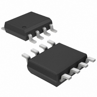
DS1338Z-18+ Maxim Integrated Products, DS1338Z-18+ Datasheet

DS1338Z-18+
Specifications of DS1338Z-18+
Related parts for DS1338Z-18+
DS1338Z-18+ Summary of contents
Page 1
... ORDERING INFORMATION DS1338Z-18+ DS1338Z-3+ DS1338Z-33+ DS1338U-18+ DS1338U-3+ DS1338U-33+ DS1338C-18# DS1338C- DS1338C-33 second line, revision level + Denotes a lead(Pb)-free/RoHS-compliant device. # Denotes a RoHS-compliant device that may include lead that is exempt under the RoHS requirements. The lead finish is JESD97 ...
Page 2
ABSOLUTE MAXIMUM RATINGS Voltage Range on Any Pin Relative to Ground………………………………………………………..……..-0.3V to +6.0V Operating Temperature Range…………………………………………………………………………..……-40°C to +85°C Storage Temperature Range………………………………………………………………………………...-55°C to +125°C ……………...……. Soldering Temperature Stresses beyond those listed under “Absolute Maximum Ratings” may cause permanent damage to the ...
Page 3
DC ELECTRICAL CHARACTERISTICS ( -40°C to +85°C, unless otherwise noted. Typical values are otherwise noted.) (Note 1) PARAMETER V Current (OSC ON 3.7V, SQW/OUT OFF (Note 7) BAT BAT V ...
Page 4
POWER-UP/POWER-DOWN CHARACTERISTICS (T = -40°C to +85°C) (Note 1, Figure 1) A PARAMETER Recovery at Power-Up (Note 15) V Fall Time PF(MAX) PF(MIN) V Rise Time PF(MIN) PF(MAX) Warning: Negative undershoots below ...
Page 5
Figure 2. Timing Diagram Figure 3. Block Diagram "C" VERSION ONLY V CC POWER GND CONTROL V BAT SERIAL BUS SCL INTERFACE AND ADDRESS SDA REGISTER 1Hz/4.096kHz/8.192kHz/32.768kHz 1Hz Oscillator and divider CONTROL LOGIC DS1338 ...
Page 6
TYPICAL OPERATING CHARACTERISTICS I vs. V BAT BAT 1250 1200 1150 1100 I BAT OSC2 SQWE = 1) 1050 ( 1000 950 900 850 800 750 700 650 600 550 1.3 1.8 2.3 2.8 3.3 3.8 4.3 4.8 5.3 V ...
Page 7
PIN DESCRIPTION PIN NAME — — BAT 4 15 GND 5 16 SDA 6 1 SCL 7 2 SQW/OUT — 4–13 N.C. DETAILED DESCRIPTION The DS1338 serial ...
Page 8
OPERATION The DS1338 operates as a slave device on the serial bus. Access is obtained by implementing a START condition and providing a device identification code, followed by data. Subsequent registers can be accessed sequentially until a STOP condition is ...
Page 9
CLOCK ACCURACY The accuracy of the clock is dependent upon the accuracy of the crystal and the accuracy of the match between the capacitive load of the oscillator circuit and the capacitive load for which the crystal was trimmed. Crystal ...
Page 10
Write transfers occur on the acknowledge from the DS1338. Once the countdown chain is reset, to avoid rollover issues the remaining time and date registers must be written within 1 second. The 1Hz square-wave ...
Page 11
CONTROL REGISTER (07H) The control register controls the operation of the SQW/OUT pin and provides oscillator status. Bit # BIT 7 BIT 6 Name OUT 0 POR 1 0 Bit 7: Output Control (OUT). Controls the output level of the ...
Page 12
I C SERIAL DATA BUS 2 The DS1338 supports the I C protocol. A device that sends data onto the bus is defined as a transmitter and a device receiving data is a receiver. The device that controls the ...
Page 13
Depending upon the state of the R/W bit, two types of data transfer are possible: 1) Data transfer from a master transmitter to a slave receiver. The master transmits the first byte (the slave address). Next follows a number of ...
Page 14
Figure 6. Data Write—Slave Receiver Mode <Slave Address> <Word Address (n)> S 1101000 0 A XXXXXXXX S - START MASTER TO SLAVE A - ACKNOWLEDGE (ACK STOP SLAVE TO MASTER Figure 7. Data Read (From Current Pointer Location)—Slave ...
Page 15
HANDLING, PCB LAYOUT, AND ASSEMBLY The DS1338C package contains a quartz tuning-fork crystal. Pick-and-place equipment may be used, but precautions should be taken to ensure that excessive shocks are avoided. Ultrasonic cleaning should be avoided to prevent damage to the ...
Page 16
... Maxim/Dallas Semiconductor cannot assume responsibility for use of any circuitry other than circuitry entirely embodied in a Maxim/Dallas Semiconductor product. No circuit patent licenses are implied. Maxim/Dallas Semiconductor reserves the right to change the circuitry and specifications without notice at any time The Maxim logo is a registered trademark of Maxim Integrated Products, Inc. The Dallas logo is a registered trademark of Dallas Semiconductor Corporation. DS1338 I DESCRIPTION © ...


