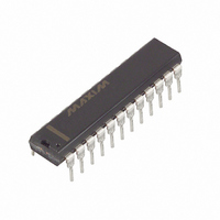
DS1642-100+ Maxim Integrated Products, DS1642-100+ Datasheet

DS1642-100+
Specifications of DS1642-100+
Related parts for DS1642-100+
DS1642-100+ Summary of contents
Page 1
... Power is Applied for the First Time UL Recognized ORDERING INFORMATION VOLTAGE PART RANGE (V) DS1642-85+ 5.0 DS1642-100+ 5.0 +Denotes a lead(Pb)-free/RoHS-compliant package. A “+" indicates a lead(Pb)-free product. The top mark will include a “+” symbol on lead-free devices. Nonvolatile Timekeeping RAM PIN CONFIGURATION TOP VIEW DQ0 DQ1 ...
Page 2
... Power-Supply Input CC DESCRIPTION The DS1642 nonvolatile static RAM and a full-function real-time clock (RTC), both of which are accessible in a bytewide format. The nonvolatile time keeping RAM is pin and function equivalent to any JEDEC-standard SRAM. The device can also be easily substituted in ROM, EPROM, and EEPROM sockets, providing read/write nonvolatility and the addition of the real-time clock function ...
Page 3
... CLOCK OPERATIONS–READING THE CLOCK While the double-buffered register structure reduces the chance of reading incorrect data, internal updates to the DS1642 clock registers should be halted before clock data is read to prevent reading of data in transition. However, halting the internal clock register updating process does not affect clock accuracy. ...
Page 4
... The 8th bit of the control register is the write bit. Setting the write bit like the read bit, halts updates to the DS1642 registers. The user can then load them with the correct day, date and time data in 24-hour BCD format. Resetting the write bit then transfers those values to the actual clock counters and allows normal operation to resume ...
Page 5
... The DS1642 has a lithium power source that is designed to provide energy for clock activity, and clock and RAM data retention when the V is sufficient to power the DS1642 continuously for the life of the equipment in which it is installed. For specification purposes, the life expectancy is 10 years at 25C with the internal clock oscillator running in the absence of V power ...
Page 6
... I/O Leakage Current (Any Output) Output Logic 1 Voltage (I = -1.0mA) OUT Output Logic 0 Voltage (I = +2.1mA) OUT Write Protection Voltage SYMBOL MIN TYP V 2 -0.3 IL SYMBOL MIN TYP CC1 I 1 CC2 2 4.25 4. DS1642 MAX UNITS NOTES MAX UNITS NOTES A +1 0 ...
Page 7
... DQ Low-Z OE Access Time OE Data Off Time OE Output Hold from Address READ CYCLE TIMING DIAGRAM 85ns ACCESS SYMBOL MIN MAX CEL t 85 CEA t 30 CEZ t 5 OEL t 45 OEA t 30 OEZ 100ns ACCESS UNITS MIN MAX 100 ns 100 100 DS1642 NOTES ...
Page 8
... Write Cycle Time Address Setup Time Pulse Width WE Pulse Width CE Data Setup Time Data Hold Time Address Hold Time Data Off Time WE Write Recovery Time 85ns ACCESS SYMBOL MIN MAX WEW t 70 CEW WEZ 100ns ACCESS UNITS MIN MAX 100 DS1642 NOTES ...
Page 9
... WRITE CYCLE TIMING DIAGRAM—WRITE-ENABLE CONTROLLED WRITE CYCLE TIMING DIAGRAM—CHIP-ENABLE CONTROLLED DS1642 ...
Page 10
... Expected Data Retention Time (Oscillator On) POWER-UP/POWER-DOWN WAVEFORM TIMING CAPACITANCE (T = +25°C) A PARAMETER Capacitance on All Pins (except DQ) Capacitance on DQ Pins SYMBOL MIN (MIN) t 300 BAT FB (MAX REC SYMBOL MIN TYP MAX UNITS NOTES s s s years TYP MAX UNITS NOTES DS1642 4, 5 ...
Page 11
... Voltages are referenced to ground. 2) Typical values are at 25C and nominal supplies. 3) Outputs are open. 4) Data retention time is at 25C. 5) Each DS1642 has a built-in switch that disconnects the lithium source until V user. The expected t is defined as a cumulative time in the absence power is first applied by the user ...
Page 12
... For the latest package outline information and land patterns www.maxim-ic.com/packages. Note that a “+”, “#”, or “-” in the package code indicates RoHS status only. Package drawings may show a different suffix character, but the drawing pertains to the package regardless of RoHS status. PACKAGE TYPE 24 EDIP DS1642 24-PIN PACKAGE PACKAGE CODE MDF24+1 PKG DIM. ...
Page 13
... Maxim cannot assume responsibility for use of any circuitry other than circuitry entirely embodied in a Maxim product. No circuit patent licenses are implied. Maxim reserves the right to change the circuitry and specifications without notice at any time Maxim is a registered trademark of Maxim Integrated Products, Inc. The Dallas logo is a registered trademark of Maxim Integrated Products, Inc. DESCRIPTION © 2010 Maxim Integrated Products DS1642 PAGES CHANGED ...


