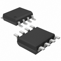
DS1340Z-18+ Maxim Integrated Products, DS1340Z-18+ Datasheet

DS1340Z-18+
Specifications of DS1340Z-18+
Related parts for DS1340Z-18+
DS1340Z-18+ Summary of contents
Page 1
... Automatic Power-Fail Detect and Switch Circuitry o Trickle-Charge Capability o Low Timekeeping Voltage Down to 1.3V o Three Operating Voltage Ranges (1.8V, 3V, and 3.3V) o Oscillator Stop Flag o Available in 8-Pin µSOP or SO Packages o Underwriters Laboratories (UL) Recognized PART DS1340Z-18+ -40°C to +85°C DS1340Z-3+ DS1340Z-33+ -40°C to +85°C DS1340U-18+ CC DS1340U-3+ DS1340U-33+ C1 DS1340C-18# -40° ...
Page 2
I C RTC with Trickle Charger ABSOLUTE MAXIMUM RATINGS Voltage Range on V Pin Relative to Ground .....-0.3V to +6.0V CC Voltage Range on SDA, SCL, and FT/OUT Relative to Ground..................................-0. Operating Temperature Range ...........................-40°C to +85°C ...
Page 3
RECOMMENDED DC OPERATING CONDITIONS ( -40°C to +85°C, unless otherwise noted. Typical values are MIN CC MAX CC A otherwise noted.) (Note 1) PARAMETER SYMBOL Supply Voltage (Note 8) Input ...
Page 4
I C RTC with Trickle Charger POWER-UP/POWER-DOWN CHARACTERISTICS (T = -40°C to +85°C) (Figure 2) A PARAMETER SYMBOL Recovery at Power-Up V Fall Time PF(MAX) V PF(MIN) V Rise Time PF(MIN) V PF(MAX) ...
Page 5
PF(MAX) V PF(MIN) INPUTS RECOGNIZED OUTPUTS VALID Figure 2. Power-Up/Power-Down Timing (V = +3.3V +25°C, unless otherwise noted vs CCSA CC 250 200 150 100 50 0 1.0 ...
Page 6
I C RTC with Trickle Charger PIN NAME 8 16 Connections for a Standard 32.768kHz Quartz Crystal. The internal oscillator circuitry is designed for 1 — X1 operation with a crystal having a specified load capacitance (C and can ...
Page 7
V drops below V CC BACKUP maintained from the V BACKUP returned to nominal levels (Table 1). After V above V , read and write access is allowed t PF Oscillator Circuit The DS1340 uses an external 32.768kHz crystal. ...
Page 8
I C RTC with Trickle Charger X1 X2 "C" VERSION ONLY BACKUP SCL SDA Figure 5. Functional Diagram Address Map Table 3 shows the DS1340 address map. The RTC reg- isters are located in address locations ...
Page 9
The day-of-week register increments at midnight. Values that correspond to the day of week are user-defined but must be sequential (i.e equals Sunday, then 2 equals Monday, and so on). Illogical time and date ...
Page 10
I C RTC with Trickle Charger Table 4. Trickle-Charge Register TCS3 TCS2 TCS1 ...
Page 11
Negative calibration blanks 128 cycles of the 32,768Hz oscillator, slowing the clock down. Positive calibration inserts 256 cycles of the 32,768Hz oscillator, speeding the clock up binary 1 ...
Page 12
I C RTC with Trickle Charger determined by the master device. The information is transferred byte-wise and each receiver acknowledges with a ninth bit. Acknowledge: Each receiving device, when addressed, is obliged to generate an acknowl- edge after the ...
Page 13
ADDRESS> <R/W> <WORD ADDRESS (n)> S 1101000 0 A XXXXXXXX S - START MASTER TO SLAVE A - ACKNOWLEDGE (ACK STOP R/W - READ/WRITE OR DIRECTION BIT ADDRESS Figure 8. Data Write—Slave Receiver Mode <SLAVE ADDRESS> <R/W> ...
Page 14
I C RTC with Trickle Charger Handling, PC Board Layout, and Assembly The DS1340C package contains a quartz tuning-fork crystal. Pick-and-place equipment may be used, but precautions should be taken to ensure that excessive shocks are avoided. Exposure to ...
Page 15
REVISION REVISION NUMBER DATE 0 6/03 Initial release. Changed “2-wire” to “I Added UL recognition info bullet to the Features section and to the V description. Added the “I/O Capacitance (SCL, SDA)” parameter (C 1 7/04 Characteristics table. Added “SDA, ...
Page 16
... Maxim cannot assume responsibility for use of any circuitry other than circuitry entirely embodied in a Maxim product. No circuit patent licenses are implied. Maxim reserves the right to change the circuitry and specifications without notice at any time. 16 ____________________Maxim Integrated Products, 120 San Gabriel Drive, Sunnyvale, CA 94086 408-737-7600 © 2010 Maxim Integrated Products is a registered trademark of Maxim Integrated Products, Inc ...


