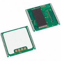
DS1743P-100+ Maxim Integrated Products, DS1743P-100+ Datasheet

DS1743P-100+
Specifications of DS1743P-100+
Related parts for DS1743P-100+
DS1743P-100+ Summary of contents
Page 1
... CE2 A11 A10 DQ7 DQ0 11 18 DQ6 DQ1 12 17 DQ5 DQ2 13 16 DQ4 GND 14 15 DQ3 28-Pin Encapsulated Package (28 PIN 740 DS1743P GND BAT 34-Pin PowerCap Module Board (Uses DS9034PCX PowerCap) : 090407 REV N.C. N.C. N.C. N.C. A12 A11 A10 A9 A8 ...
Page 2
... DQ0 12 15 DQ1 13 14 DQ2 14 17 GND 15 13 DQ3 16 12 DQ4 17 11 DQ5 18 10 DQ6 19 9 DQ7 DS1743/DS1743P Y2K-Compliant, Nonvolatile Timekeeping RAMs FUNCTION PDIP No Connection Address Input Data Input/ Output — Ground — Data Input/ — Output PIN NAME FUNCTION PowerCap ...
Page 3
... DS1743-85+ 0°C to +70°C DS1743-100+ 0°C to +70°C DS1743-100 IND+ -40°C to +85°C DS1743P-85+ 0°C to +70°C DS1743P-100+ 0°C to +70°C DS1743P-100IND+ -40°C to +85°C DS1743W-120+ 0°C to +70°C DS1743W-120 IND+ -40°C to +85°C DS1743W-150+ 0°C to +70°C DS1743W-150 IND+ -40° ...
Page 4
... This design allows the PowerCap to be mounted on top of the DS1743P after the completion of the surface-mount process. Mounting the PowerCap after the surface- mount process prevents damage to the crystal and battery due to the high temperatures required for solder reflow ...
Page 5
... LSB of the seconds register will toggle at 512Hz. When the seconds register is being read, the DQ0 line will toggle at the 512Hz frequency as long as conditions for access remain valid (i.e., CE low, OE low, WE high, and address for seconds register remain valid and stable). DS1743/DS1743P Y2K-Compliant, Nonvolatile Timekeeping RAMs Dallas Semiconductor DS1743 ...
Page 6
... AA changed while CE and OE remain valid, output data will remain valid for output data hold time (t will then go indeterminate until the next address access. DS1743/DS1743P Y2K-Compliant, Nonvolatile Timekeeping RAMs DATA ...
Page 7
... This bit is not writeable and should always when read ever present, an exhausted lithium energy source is indicated and both the contents of the RTC and RAM are questionable. DS1743/DS1743P Y2K-Compliant, Nonvolatile Timekeeping RAMs WR prior to the end of write and remain valid for t ...
Page 8
... Output Leakage Current (Any Output) Output Logic 1 Voltage (I = -1.0mA) OUT Output Logic 0 Voltage (I = 2.1mA) OUT Write-Protection Voltage Battery Switchover Voltage DS1743/DS1743P Y2K-Compliant, Nonvolatile Timekeeping RAMs TEMP RANGE 3.3V 10 10% 0°C to +70°C 3.3V 10 10% -40C to +85C SYMBOL CONDITIONS = 5V 10 ...
Page 9
... Over the Operating Range PARAMETER SYMBOL Read Cycle Time Address Access Time CE to CE2 to DQ Low-Z CE Access Time CE2 Access Time CE and CE2 Data-Off Time Low-Z OE Access Time OE Data-Off Time Output Hold from Address DS1743/DS1743P Y2K-Compliant, Nonvolatile Timekeeping RAMs SYMBOL MIN CC1 I CC2 ...
Page 10
... Address Access Time CE and CE2 Low to DQ Low-Z CE and CE2 Access Time CE and CE2 Data-Off time OE Low to DQ Low-Z OE Access Time OE Data-Off Time Output Hold from Address READ CYCLE TIMING DIAGRAM DS1743/DS1743P Y2K-Compliant, Nonvolatile Timekeeping RAMs ACCESS 120ns SYMBOL MIN MAX MIN t 120 ...
Page 11
... PARAMETER Write Cycle Time Address Setup Time WE Pulse Width CE and CE2 Pulse Width Data Setup Time Data Hold Time CE Data Hold Time CE2 Address Hold Time WE Data-Off Time Write Recovery Time DS1743/DS1743P Y2K-Compliant, Nonvolatile Timekeeping RAMs ACCESS 70ns MIN MAX MIN ...
Page 12
... WRITE CYCLE TIMING—WRITE-ENABLE CONTROLLED (See Note 5) WRITE CYCLE TIMING— CE /CE2-CONTROLLED (See Note 5) DS1743/DS1743P Y2K-Compliant, Nonvolatile Timekeeping RAMs ...
Page 13
... CE2 Before IH IL Power-Down V Fall Time PF(MAX) PF(MIN) V Fall Time PF(MIN Rise Time PF(MIN) PF(MAX) Power-Up Recover Time Expected Data-Retention Time (Oscillator On) POWER-UP/DOWN TIMING (5V DEVICE) DS1743/DS1743P Y2K-Compliant, Nonvolatile Timekeeping RAMs SYMBOL MIN TYP 300 REC MAX UNITS NOTES s s s ...
Page 14
... PF(MIN) V Rise Time PF(MIN) PF(MAX) to RST High V PF Expected Data-Retention Time (Oscillator On) POWER-UP/DOWN WAVEFORM TIMING (3.3V DEVICE) CAPACITANCE (T = +25C) A PARAMETER Capacitance on All Input Pins Capacitance on All Output Pins DS1743/DS1743P Y2K-Compliant, Nonvolatile Timekeeping RAMs SYMBOL MIN TYP 300 REC SYMBOL MIN ...
Page 15
... Post-solder cleaning with water-washing techniques is acceptable, provided that ultrasonic vibration is not used. See the PowerCap package drawing for details regarding the PowerCap package. DS1743/DS1743P Y2K-Compliant, Nonvolatile Timekeeping RAMs applies ...
Page 16
... No circuit patent licenses are implied. Maxim/Dallas Semiconductor reserves the right to change the circuitry and specifications without notice at any time The Maxim logo is a registered trademark of Maxim Integrated Products, Inc. The Dallas logo is a registered trademark of Dallas Semiconductor. DS1743/DS1743P Y2K-Compliant, Nonvolatile Timekeeping RAMs DOCUMENT NO. 21-0245 ...


