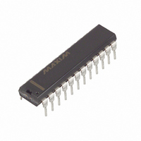
DS1742-100+ Maxim Integrated Products, DS1742-100+ Datasheet

DS1742-100+
Specifications of DS1742-100+
Related parts for DS1742-100+
DS1742-100+ Summary of contents
Page 1
... GND DQ3 ENCAPSULATED DIP PIN-PACKAGE TOP MARK** 24 EDIP (0.740a) DS1742-85 24 EDIP (0.740a) DS1742-85+ 24 EDIP (0.740a) DS1742-100 24 EDIP (0.740a) DS1742-100+ 24 EDIP (0.740a) DS1742-100IND 24 EDIP (0.740a) DS1742-100IND+ 24 EDIP (0.740a) DS1742W-120 24 EDIP (0.740a) DS1742W-120+ 24 EDIP (0.740a) DS1742W-150 24 EDIP (0.740a) DS1742W-150+ REV: 102808 RAM ...
Page 2
... DESCRIPTION The DS1742 is a full-function, year 2000-compliant (Y2KC), real-time clock/calendar (RTC) and nonvolatile static RAM. User access to all registers within the DS1742 is accomplished with a bytewide interface as shown in Figure 1. The RTC information and control bits reside in the eight uppermost RAM locations. The RTC registers contain century, year, month, date, day, hours, minutes, and seconds data in 24-hour BCD format ...
Page 3
... CLOCK OPERATIONS—READING THE CLOCK While the double-buffered register structure reduces the chance of reading incorrect data, internal updates to the DS1742 clock registers should be halted before clock data is read to prevent reading of data in transition. However, halting the internal clock register updating process does not affect clock accuracy. Updating is halted when written into the read bit, bit 6 of the century register, see Table 2 ...
Page 4
... As shown in Table 2, bit 7 of the century register is the write bit. Setting the write bit like the read bit, halts updates to the DS1742 registers. The user can then load them with the correct day, date and time data in 24-hour BCD format. Resetting the write bit then transfers those values to the actual clock counters and allows normal operation to resume ...
Page 5
... RETRIEVING DATA FROM RAM OR CLOCK The DS1742 is in the read mode wheneve high, and (chip enable) is low. The device architecture allows ripple-through access to any CE of the address locations in the NV SRAM. Valid data will be available at the DQ pins within t after the last address input is stable, providing that the satisfied ...
Page 6
... BATTERY LONGEVITY The DS1742 has a lithium power source that is designed to provide energy for clock activity, and clock and RAM data retention when the V internal power supply is sufficient to power the DS1742 continuously for the life of the equipment in which it is installed. For specification purposes, the life expectancy is 10 years at 25° ...
Page 7
... Battery Switchover Voltage TEMPERATURE 0°C to +70°C (noncondensing) -40°C to +85°C (noncondensing) SYMBOL MIN TYP -0.3 IL SYMBOL MIN CC1 I CC2 2 4. 3.3V 10 10% 3.3V ±10 ±10% MAX UNITS NOTES +0.8 V +0.6 V TYP MAX UNITS 0.4 4. BAT DS1742 NOTES ...
Page 8
... Output Hold from Address SYMBOL MIN CC1 I CC2 2 2. 85ns ACCESS SYMBOL MIN MAX CEL t 85 CEA t 30 CEZ t 5 OEL t 45 OEA t 30 OEZ TYP MAX UNITS 0 0 0.4 2. BAT 100ns ACCESS UNITS MIN MAX 100 ns 100 100 DS1742 NOTES ...
Page 9
... Access Time OE Data Off Time OE Output Hold from Address READ CYCLE TIMING DIAGRAM 120ns ACCESS SYMBOL MIN MAX t 120 RC t 120 CEL t 120 CEA t 40 CEZ t 5 OEL t 100 OEA t 35 OEZ 150ns ACCESS UNITS MIN MAX 150 ns 150 150 130 DS1742 ...
Page 10
... Address Hold Time Data Off Time WE Write Recovery Time 85ns ACCESS MIN MAX WEW t 70 CEW WEZ 120ns SYMBOL ACCESS MIN MAX t 120 100 WEW t 110 CEW WEZ 100ns ACCESS UNITS MIN MAX 100 150ns ACCESS UNITS MIN MAX 150 130 ns 140 DS1742 ...
Page 11
... WRITE CYCLE TIMING DIAGRAM—WRITE-ENABLE CONTROLLED WRITE CYCLE TIMING DIAGRAM—CHIP-ENABLE CONTROLLED DS1742 ...
Page 12
... CC PARAMETER Before Power-Down Fall Time PF(MAX) V Fall Time PF(MIN) V Rise Time PF(MIN) Power-Up Recover Time Expected Data Retention Time (Oscillator On) POWER-UP/POWER-DOWN WAVEFORM TIMING (5V DEVICE) SYMBOL MIN 300 PF(MIN PF(MAX REC TYP MAX UNITS s 0 s s 10 years DS1742 NOTES 5, 6 ...
Page 13
... Expected Data Retention Time (Oscillator On) POWER-UP/POWER-DOWN WAVEFORM TIMING (3.3V DEVICE) CAPACITANCE (T = +25°C) A PARAMETER Capacitance on All Input Pins Capacitance on All Output Pins SYMBOL MIN 300 PF(MIN PF(MAX REC SYMBOL MIN TYP MAX UNITS years TYP MAX UNITS DS1742 NOTES 5, 6 NOTES ...
Page 14
... Outputs are open. 4) Battery switchover occurs at the lower of either the battery voltage Data retention time is at 25°C. 6) Each DS1742 has a built-in switch that disconnects the lithium source until V applied by the user. The expected t starting from the time power is first applied by the user. ...
Page 15
PACKAGE INFORMATION For the latest package outline information and land patterns www.maxim-ic.com/packages. PACKAGE TYPE PACKAGE CODE 24 EDIP MDF24+1 DOCUMENT NO. 21-0245 ...
Page 16
... Ordering Information table. Removed reference to J-STD-020 and indicated the lead 060706 soldering temperature of +260C for 10 seconds max. Added DS1742-85, DS1742-85+ to the Ordering Information 022207 table; removed DS1742P-100+ (PowerCap) package. Removed the –70 ordering numbers from the Ordering 102808 Information table. ...


