DS1553P-100+ Maxim Integrated Products, DS1553P-100+ Datasheet
DS1553P-100+
Specifications of DS1553P-100+


Related parts for DS1553P-100+


DS1553P-100+ Summary of contents
Page 1
... ORDERING INFORMATION PART VOLTAGE (V) DS1553-85+ 5.0 DS1553-100+ 5.0 DS1553W-120+ 3.3 DS1553W-150+ 3.3 DS1553P-85+ 5.0 DS1553P-100+ 5.0 DS1553WP-120+ 3.3 DS1553WP-150+ 3.3 DS9034PCX Denotes a lead(Pb)-free/RoHS-compliant package. * PowerCap required, must be ordered separately **A “+” symbol anywhere on the top mark indicates a lead(Pb)-free package. ...
Page 2
PIN DESCRIPTION PIN NAME EDIP PowerCap RST A12 A10 23 ...
Page 3
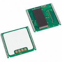
... The 34-pin PowerCap module board is designed with contacts for connection to a separate PowerCap (DS9034PCX) that contains the crystal and battery. This design allows the PowerCap to be mounted on top of the DS1553P after completion of the surface-mount process. Mounting the PowerCap after the surface-mount process prevents damage to the crystal and battery due to the high temperatures required for solder reflow ...
Page 4
Table 1. Operating Modes > < V < <V X BAT DATA READ MODE The DS1553 is ...
Page 5
V . RTC operation and SRAM data are maintained from the battery until V SO nominal levels. All control, data, and address signals must be powered down when V BATTERY LONGEVITY The DS1553 has a lithium power source that ...
Page 6
CLOCK OPERATIONS Table 2 and the following paragraphs describe the operation of RTC, alarm, and watchdog functions. Table 2. Register Map ADDRESS 1FFFh 10 Year 1FFEh X X 1FFDh X X 1FFCh X FT 1FFBh X ...
Page 7
READING THE CLOCK When reading the RTC data recommended to halt updates to the external set of double-buffered RTC registers. This puts the external registers into a static state, allowing data to be read without register values changing ...
Page 8
USING THE CLOCK ALARM The alarm settings and control for the DS1553 reside within registers 1FF2h–1FF5h. Register 1FF6h contains two alarm-enable bits: Alarm Enable (AE) and Alarm in Backup Enable (ABE). The AE and ABE bits must be set as ...
Page 9
Figure 2. Clearing IRQ Waveforms , CE Figure 3. Clearing IRQ Waveforms CE = Ø The /FT pin can also be activated in the battery-backed mode. The IRQ occurs and both ABE and AE are set. The ABE and AE ...
Page 10
USING THE WATCHDOG TIMER The watchdog timer can be used to detect an out-of-control processor. The user programs the watchdog timer by setting the desired amount of timeout into the 8-bit Watchdog register (Address 1FF7h). The five Watchdog register bits ...
Page 11
ABSOLUTE MAXIMUM RATINGS Voltage Range on Any Pin Relative to Ground……………………………………………..-0.3V to +6.0V Storage Temperature Range EDIP .......................………………………………………………………………..-40C to +85C PowerCap...............………………………………………………………………..-55C to +125C Lead Temperature (soldering, 10s)…………………………….........................................................+260°C (Note: EDIP is hand or wave-soldered only.) (Note 8) Soldering Temperature (reflow)……………………………………..................................................+260°C This ...
Page 12
DC ELECTRICAL CHARACTERISTICS (V = 3.3V ±10 Over the operating range PARAMETER Active Supply Current TTL Standby Current ( CMOS Standby Current (CE 0.2V) CC Input Leakage Current (Any Input) ...
Page 13
READ CYCLE, AC CHARACTERISTICS (V = 5.0V ± Over the operating range PARAMETER Read Cycle Time Address Access Time Low-Z CE Access Time CE Data Off Time Low-Z ...
Page 14
WRITE CYCLE, AC CHARACTERISTICS (V = 5.0V ±10 Over the operating range PARAMETER Write Cycle Time Address Access Time WE Pulse Width CE Pulse Width Data Setup Time Data Hold time Address Hold Time WE Data ...
Page 15
Figure 6. Write Cycle Timing, Write-Enable Controlled Figure 7. Write Cycle Timing, Chip-Enable Controlled ...
Page 16
POWER-UP/DOWN CHARACTERISTICS (V = 5.0V ± Over the operating range PARAMETER Before Power-Down IH V Fall Time PF(MAX) PF(MIN) V Fall Time ...
Page 17
POWER-UP/DOWN CHARACTERISTICS (V = 3.3V ± Over the operating range PARAMETER Before Power-Down IH V Fall Time PF(MAX) PF(MIN) V Rise Time ...
Page 18
AC TEST CONDITIONS Output Load: 100 pF + 1TTL Gate Input Pulse Levels 3.0V Timing Measurement Reference Levels: Input: 1.5V Output: 1.5V Input Pulse Rise and Fall Times: 5ns NOTES: 1) Voltage referenced to ground. 2) Typical values ...
Page 19
PIN CONFIGURATIONS TOP VIEW RST 1 A12 2 DS1553 DQ0 11 DQ1 12 13 DQ2 14 GND 28-Pin Encapsulated Package (700-mil Extended) PACKAGE INFORMATION ...
Page 20
... Maxim Integrated Products DS1553 64kB, Nonvolatile, Year-2000-Compliant Timekeeping RAM DESCRIPTION ; changed 70ns Access to 85ns Access in the Write OEZ , t , and t ; updated the Package Information table and DS WEZ Maxim and the Dallas logo are registered trademarks of Maxim Integrated Products, Inc. PAGES CHANGED , 13, 14, 19 ...