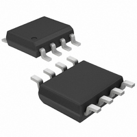
DS1307Z+T&R Maxim Integrated Products, DS1307Z+T&R Datasheet

DS1307Z+T&R
Specifications of DS1307Z+T&R
Related parts for DS1307Z+T&R
DS1307Z+T&R Summary of contents
Page 1
GENERAL DESCRIPTION The DS1307 serial real-time clock (RTC low- power, full binary-coded decimal (BCD) clock/calendar plus 56 bytes of NV SRAM. Address and data are transferred serially through an I The clock/calendar provides seconds, minutes, hours, day, date, ...
Page 2
ABSOLUTE MAXIMUM RATINGS Voltage Range on Any Pin Relative to Ground ................................................................................ -0.5V to +7.0V Operating Temperature Range (Noncondensing) Commercial .......................................................................................................................... 0°C to +70°C Industrial ............................................................................................................................ -40°C to +85°C Storage Temperature Range ......................................................................................................... -55°C to +125°C Soldering Temperature (DIP, leads) ...
Page 3
AC ELECTRICAL CHARACTERISTICS (V = 4.5V to 5.5V 0°C to +70° PARAMETER SCL Clock Frequency Bus Free Time Between a STOP and START Condition Hold Time (Repeated) START Condition LOW Period of SCL Clock HIGH ...
Page 4
TIMING DIAGRAM SDA t BUF t LOW SCL t HD:STA STOP START Figure 1. Block Diagram POWER GND CONTROL V BAT SERIAL BUS SCL INTERFACE AND ADDRESS SDA REGISTER DS1307 64 x ...
Page 5
TYPICAL OPERATING CHARACTERISTICS (V = 5.0V +25°C, unless otherwise noted vs. V CCS CC 120 110 100 1.0 2.0 3.0 4 ...
Page 6
PIN DESCRIPTION PIN NAME Connections for Standard 32.768kHz Quartz Crystal. The internal oscillator circuitry is designed for operation with a crystal having a specified load capacitance ( the input to the oscillator and can optionally be ...
Page 7
OSCILLATOR CIRCUIT The DS1307 uses an external 32.768kHz crystal. The oscillator circuit does not require any external resistors or capacitors to operate. Table 1 specifies several crystal parameters for the external crystal. Figure 1 shows a functional schematic of the ...
Page 8
CLOCK AND CALENDAR The time and calendar information is obtained by reading the appropriate register bytes. Table 2 shows the RTC registers. The time and calendar are set or initialized by writing the appropriate register bytes. The contents of the ...
Page 9
CONTROL REGISTER The DS1307 control register is used to control the operation of the SQW/OUT pin. BIT 7 BIT 6 BIT 5 OUT 0 Bit 7: Output Control (OUT). This bit controls the output level of the SQW/OUT pin when ...
Page 10
I C DATA BUS 2 The DS1307 supports the I C protocol. A device that sends data onto the bus is defined as a transmitter and a device receiving data as a receiver. The device that controls the message ...
Page 11
Figure 3. Data Transfer on I SDA MSB SCL 1 2 START CONDITION Depending upon the state of the R/W bit, two types of data transfer are possible: 1. Data transfer from a master transmitter to a slave receiver. The ...
Page 12
The DS1307 can operate in the following two modes: 1. Slave Receiver Mode (Write Mode): Serial data and clock are received through SDA and SCL. After each byte is received an acknowledge bit is transmitted. START and STOP conditions are ...
Page 13
Figure 6. Data Read (Write Pointer, Then Read)—Slave Receive and Transmit <Slave Address> <Word Address (n)> XXXXXXXX A 1101000 <Data(n)> <Data(n+1)> XXXXXXXX A XXXXXXXX A XXXXXXXX S - Start Sr - Repeated Start Master to slave A ...
Page 14
... Maxim cannot assume responsibility for use of any circuitry other than circuitry entirely embodied in a Maxim product. No circuit patent licenses are implied. Maxim reserves the right to change the circuitry and specifications without notice at any time © 2008 Maxim Integrated Products DS1307 Serial, I DESCRIPTION Maxim is a registered trademark of Maxim Integrated Products, Inc Real-Time Clock PAGES CHANGED 1 1 ...


