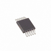
DS1390U-18+ Maxim Integrated Products, DS1390U-18+ Datasheet

DS1390U-18+
Specifications of DS1390U-18+
Related parts for DS1390U-18+
DS1390U-18+ Summary of contents
Page 1
... Three Operating Voltages: 1.8V ±5%, 3.0V ±10%, and 2.97 to 5.5V (DS1394: 3.3V ±10%) ♦ Industrial Temperature Range: -40°C to +85°C ♦ Underwriters Laboratories (UL) Recognized PART DS1390U-18+ DS1390U-3+ DS1390U-33+ DS1390U-33/V+ DS1391U-18+ DS1391U-3+ DS1391U-33+ ...
Page 2
Low-Voltage SPI/3-Wire RTCs with Trickle Charger ABSOLUTE MAXIMUM RATINGS Voltage Range on V Pin Relative to Ground .....-0.3V to +6.0V CC Voltage Range on Inputs Relative to Ground ...............................................-0. Operating Temperature Range ...........................-40°C to +85°C Stresses beyond those ...
Page 3
Low-Voltage SPI/3-Wire RTCs with RECOMMENDED DC OPERATING CONDITIONS (continued -40°C to +85°C, unless otherwise noted. Typical values are at nominal supply voltage and T CC CC(MIN) CC(MAX) A unless otherwise noted.) (Note ...
Page 4
Low-Voltage SPI/3-Wire RTCs with Trickle Charger SCLK CDH t DC W/R DIN DOUT CPHA = 1 NOTE: SCLK CAN BE EITHER POLARITY SHOWN FOR CPOL = 1. Figure 1a. Timing Diagram—SPI Read ...
Page 5
Low-Voltage SPI/3-Wire RTCs with CPHA = SCLK t CDH t DC DIN W/R WRITE ADDRESS BYTE DOUT NOTE: SCLK CAN BE EITHER POLARITY SHOWN FOR CPOL = 1. Figure 2a. Timing Diagram—SPI ...
Page 6
Low-Voltage SPI/3-Wire RTCs with Trickle Charger AC ELECTRICAL CHARACTERISTICS—3-WIRE INTERFACE ( -40°C to +85°C.) (Note 1) (Figures CC(MIN) CC(MAX) A PARAMETER SYMBOL SCLK Frequency (Note 13) f Data to SCLK ...
Page 7
Low-Voltage SPI/3-Wire RTCs with SCLK CDH t DC I/O A0 WRITE ADDRESS BYTE Figure 3. Timing Diagram—3-Wire Read Transfer SCLK CDH t DC I/O A0 WRITE ...
Page 8
Low-Voltage SPI/3-Wire RTCs with Trickle Charger POWER-UP/POWER-DOWN CHARACTERISTICS (T = -40°C to +85°C) (Figures PARAMETER SYMBOL V Detect to Recognize Inputs CC (V Rising Fall Time PF(MAX) V PF(MIN) V Rise Time; ...
Page 9
Low-Voltage SPI/3-Wire RTCs with CAPACITANCE (T = +25°C) A PARAMETER SYMBOL Capacitance on All Input Pins Capacitance on All Output Pins (High Impedance) WARNING: Negative undershoots below -0.3V while the part is in battery-backed mode can cause loss of data. ...
Page 10
Low-Voltage SPI/3-Wire RTCs with Trickle Charger (V = +3.3V +25°C, unless otherwise noted vs BBSQ1 = 0 BACKUP BACKUP 600 550 500 450 400 350 300 1.3 1.7 2.1 2.5 2.9 3.3 3.7 ...
Page 11
Low-Voltage SPI/3-Wire RTCs with PIN DS1390/ DS1391 DS1392 DS1393 DS1394 — — — — — — — — ...
Page 12
Low-Voltage SPI/3-Wire RTCs with Trickle Charger LEVEL DETECT, CC POWER SWITCH, GND WRITE PROTECT, TRICKLE CHARGER V BACKUP (DS1390/91/94) CS (DS1392/93) (CE) SCLK BUS (DS1390/91/94) DIN INTERFACE (DS1390/91/94) DOUT (DS1392/93) I/O ...
Page 13
Low-Voltage SPI/3-Wire RTCs with Power Control The power-control function is provided by a precise, temperature-compensated voltage reference and a comparator circuit that monitors the V device is fully accessible and data can be written and read when V is greater ...
Page 14
Low-Voltage SPI/3-Wire RTCs with Trickle Charger Address Map Table 3 shows the address map for the DS1390– DS1393 RTC and RAM registers. The RTC registers are located in address locations 00h to 0Fh in read mode, and 80h to 8Fh ...
Page 15
Low-Voltage SPI/3-Wire RTCs with Table 3. Address Map (continued) WRITE READ BIT 7 BIT 6 ADDRESS ADDRESS 8Bh 0Bh AM3 12/24 8Ch 0Ch AM4 DY/DT 0 EOSC 8Dh 0Dh 0 0 8Eh 0Eh OSF 0 8Fh 0Fh TCS3 TCS2 Note: ...
Page 16
Low-Voltage SPI/3-Wire RTCs with Trickle Charger All five devices contain one time-of-day/date alarm. Writing to registers 88h through 8Ch sets the alarm. The alarm can be programmed (by the alarm enable and INTCN bits of the control register) to activate ...
Page 17
Low-Voltage SPI/3-Wire RTCs with Special-Purpose Registers The DS1390–DS1394 have three additional registers (control, status, and trickle charger) that control the RTC, alarms, square-wave output, and trickle charger. BIT 7 BIT 6 BIT 5 EOSC 0 BBSQI Bit 7: Enable Oscillator ...
Page 18
Low-Voltage SPI/3-Wire RTCs with Trickle Charger BIT 7 BIT 6 BIT 5 EOSC 0 BBSQI The INTCN bit used in the DS1390/DS1393/DS1394 becomes the SQW pin-enable bit in the DS1392. This BIT 7 BIT 6 BIT 5 OSF 0 Bit ...
Page 19
Low-Voltage SPI/3-Wire RTCs with TRICKLE-CHARGE REGISTER (8Fh WRITE, 0Fh READ) BIT 6 BIT 5 BIT 4 BIT 7 TCS3 TCS2 TCS1 TCS0 SELECT NOTE: ONLY 1010b ENABLES CHARGER V CC Figure 8. DS1390–DS1394 Programmable Trickle Charger Table ...
Page 20
Low-Voltage SPI/3-Wire RTCs with Trickle Charger SPI Serial-Data Bus The DS1390/DS1391/DS1394 provide a 4-wire SPI seri- al-data bus to communicate in systems with an SPI host controller. The DS1390/DS1391 support SPI modes 1 and 3, while the DS1394 supports SPI ...
Page 21
Low-Voltage SPI/3-Wire RTCs with CS SCLK (MODE 0) SCLK (MODE 1) DIN W DOUT Figure 10. SPI Single-Byte Write CS SCLK (MODE 0) SCLK (MODE 1) DIN W HIGH IMPEDANCE DOUT Figure 11. SPI ...
Page 22
Low-Voltage SPI/3-Wire RTCs with Trickle Charger CS SCLK DIN WRITE ADDRESS BYTE DIN ADDRESS BYTE READ DOUT HIGH-IMPEDANCE Figure 12. SPI Multiple-Byte Burst Transfer CE SCLK I Figure 13. 3-Wire Single-Byte Read CE SCLK I/O A1 ...
Page 23
Low-Voltage SPI/3-Wire RTCs with 3-Wire Serial-Data Bus The DS1392/DS1393 provide a 3-wire serial-data bus, and support both single-byte and multiple-byte data transfers for maximum flexibility. The I/O pin is the seri- al-data input/output pin. The CE input is used to ...
Page 24
Low-Voltage SPI/3-Wire RTCs with Trickle Charger TOP VIEW DS1390 BACKUP DS1394 GND μSOP DS1392 V 3 BACKUP GND μSOP 24 ____________________________________________________________________ ...
Page 25
Low-Voltage SPI/3-Wire RTCs with CRYSTAL SCLK CPU DS1390/ DOUT DS1394 DIN GND CRYSTAL SCLK CPU DS1392 I/O GND For the latest package outline information and land patterns www.maxim-ic.com/packages. ...
Page 26
... Added DS1390U-33/V+ to the Ordering Information table. Maxim cannot assume responsibility for use of any circuitry other than circuitry entirely embodied in a Maxim product. No circuit patent licenses are implied. Maxim reserves the right to change the circuitry and specifications without notice at any time. ...


