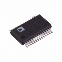
AD9201ARSZ Analog Devices Inc, AD9201ARSZ Datasheet

AD9201ARSZ
Specifications of AD9201ARSZ
Available stocks
Related parts for AD9201ARSZ
AD9201ARSZ Summary of contents
Page 1
FEATURES Complete Dual Matching ADCs Low Power Dissipation: 215 mW (+3 V Supply) Single Supply: 2 5.5 V Differential Nonlinearity Error: 0.4 LSB On-Chip Analog Input Buffers On-Chip Reference Signal-to-Noise Ratio: 57.8 dB Over Nine Effective Bits ...
Page 2
AD9201–SPECIFICATIONS Parameter RESOLUTION CONVERSION RATE DC ACCURACY Differential Nonlinearity Integral Nonlinearity Differential Nonlinearity (SE) Integral Nonlinearity (SE) Zero-Scale Error, Offset Error Full-Scale Error, Gain Error Gain Match Offset Match ANALOG INPUT Input Voltage Range Input Capacitance Aperture Delay Aperture Uncertainty ...
Page 3
Parameter 3 DYNAMIC PERFORMANCE (SE) Signal-to-Noise and Distortion f = 3.58 MHz Signal-to-Noise f = 3.58 MHz Total Harmonic Distortion f = 3.58 MHz Spurious Free Dynamic Range f = 3.58 MHz DIGITAL INPUTS High Input Voltage Low Input Voltage ...
Page 4
AD9201 ABSOLUTE MAXIMUM RATINGS* With Respect Parameter to Min AVDD AVSS –0.3 DVDD DVSS –0.3 AVSS DVSS –0.3 AVDD DVDD –6.5 CLK AVSS –0.3 Digital Outputs DVSS –0.3 AINA, AINB AVSS –1.0 VREF AVSS –0.3 REFSENSE AVSS –0.3 REFT, REFB ...
Page 5
AVDD DRVDD DRVSS AVSS a. D0–D9, OTR AVDD AVDD IN AVSS AVSS d. INA, INB OFFSET ERROR The first transition should occur at a level 1 LSB above “zero.” Offset is defined as the deviation of the actual first code ...
Page 6
Characteristic Curves AD9201 (AVDD = +3 V, DVDD = + MHz (50% duty cycle input span from –0 +1 internal reference unless otherwise noted) 1.5 1.0 0.5 ...
Page 7
CLOCK FREQUENCY – Hz Figure 9. THD vs. Clock Frequency (f 1.012 1.011 1.010 1.009 1.008 1.007 1.006 –40 – TEMPERATURE – C Figure 10. Voltage Reference Error vs. ...
Page 8
AD9201 10 FUND 0 –10 –20 –30 –40 –50 –60 –70 2ND 4TH 3RD –80 –90 –100 –110 –120 0.0E+0 1.0E+6 2.0E+6 3.0E+6 4.0E+6 5.0E+6 6.0E+6 7.0E+6 8.0E+6 9.0E+6 10.0E+6 10 FUND 0 –10 –20 –30 –40 –50 –60 5TH ...
Page 9
The AD9201 can accommodate a variety of input spans be- tween 1 V and 2 V. For spans of less than 1 V, expect a propor- tionate degradation in SNR . Use span will provide the ...
Page 10
AD9201 REFERENCE AND REFERENCE BUFFER The reference and buffer circuitry on the AD9201 is configured for maximum convenience and flexibility. An illustration of the equivalent reference circuit is show in Figure 26. The user can select from five different reference ...
Page 11
ADC CORE 0.1 F IREFT 10 F 0.1 F IREFB 1V 0.1 F VREF 10 F 0.1 F 10k REFSENSE INTERNAL CONTROL 10k LOGIC AVSS AD9201 Figure 26. Reference Buffer Equivalent Circuit and Exter- nal Decoupling Recommendation For best results ...
Page 12
AD9201 COMMON-MODE PERFORMANCE Attention to the common-mode point of the analog input volt- age can improve the performance of the AD9201. Figure 29 illustrates THD as a function of common-mode voltage (center point of the analog input span) and power ...
Page 13
DIGITAL INPUTS AND OUTPUTS Each of the AD9201 digital control inputs, CHIP SELECT, CLOCK, SELECT and SLEEP are referenced to AVDD and AVSS. Switching thresholds will be AVDD/2. The format of the digital output is straight binary. A low power ...
Page 14
AD9201 At the receiver, the demodulation of a QAM signal back into its separate I and Q components is essentially the modulation pro- cess explain above but in the reverse order. A common and traditional implementation of a QAM demodulator ...
Page 15
EVALUATION BOARD The AD9201 evaluation board is shipped “ready to run.” Power and signal generators should be connected as shown in Figure 35. Then the user can observe the performance of the Q channel. If the user wants to observe ...
Page 16
AD9201 Figure 36. Evaluation Board Solder-Side Silkscreen (NOT TO SCALE) Figure 37. Evaluation Board Component-Side Layout R50 R51 C50 C14 C51 C14 C20 C17 C22 C23 C27 C24 C53 R52 R53 (NOT TO SCALE) –16– REV. D ...
Page 17
TO SCALE) Figure 38. Evaluation Board Ground Plane Layout (NOT TO SCALE) REV. D Figure 39. Evaluation Board Solder-Side Layout –17– AD9201 ...
Page 18
AD9201 I_IN AGND J1 AVDD TP3 AGND J4 Q_IN (NOT TO SCALE) Figure 40. Evaluation Board Component-Side Silkscreen (NOT TO SCALE) STROBE AGND AVDD CLOCK BJ1 C40 BJ2 J5 J6 C42 + R38 L2 C38 C41 JP22 R37 R13 V8 ...
Page 19
REV. D Figure 42. Evaluation Board –19– AD9201 ...
Page 20
AD9201 0.078 (1.98) 0.068 (1.73) 0.008 (0.203) 0.002 (0.050) OUTLINE DIMENSIONS Dimensions shown in inches and (mm). 28-Lead Shrink Small Outline Package (SSOP) (RS-28) 0.407 (10.34) 0.397 (10.08 0.07 (1.79) PIN 1 0.066 (1.67) 8 0.0256 ...


