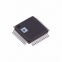
AD7663ASTZ Analog Devices Inc, AD7663ASTZ Datasheet - Page 13

AD7663ASTZ
Manufacturer Part Number
AD7663ASTZ
Description
IC ADC 16BIT CMOS 48-LQFP
Manufacturer
Analog Devices Inc
Series
PulSAR®r
Datasheet
1.AD7663ASTZ.pdf
(24 pages)
Specifications of AD7663ASTZ
Data Interface
Serial, Parallel
Number Of Bits
16
Sampling Rate (per Second)
250k
Number Of Converters
1
Power Dissipation (max)
41mW
Voltage Supply Source
Analog and Digital
Operating Temperature
-40°C ~ 85°C
Mounting Type
Surface Mount
Package / Case
48-LQFP
Resolution (bits)
16bit
Sampling Rate
250kSPS
Input Channel Type
Differential
Supply Voltage Range - Analog
4.75V To 5.25V
Lead Free Status / RoHS Status
Lead free / RoHS Compliant
For Use With
EVAL-AD7663CBZ - BOARD EVALUATION FOR AD7663
Lead Free Status / RoHS Status
Lead free / RoHS Compliant, Lead free / RoHS Compliant
Available stocks
Company
Part Number
Manufacturer
Quantity
Price
Company:
Part Number:
AD7663ASTZ
Manufacturer:
AD
Quantity:
513
Company:
Part Number:
AD7663ASTZ
Manufacturer:
Analog Devices Inc
Quantity:
10 000
Part Number:
AD7663ASTZ
Manufacturer:
ADI/亚德诺
Quantity:
20 000
Company:
Part Number:
AD7663ASTZRL
Manufacturer:
Analog Devices Inc
Quantity:
10 000
Figure 6 shows a simplified analog input section of the AD7663.
The four resistors connected to the four analog inputs form a resis-
tive scaler that scales down and shifts the analog input range to a
common input range of 0 V to 2.5 V at the input of the switched
capacitive ADC.
By connecting the four inputs INA, INB, INC, and IND to the
input signal itself, the ground, or a 2.5 V reference, other analog
input ranges can be obtained.
REV. B
ADR421
2.5V REF
NOTE 1
ANALOG
( 10V)
IND
INC
INB
INA
INPUT
Figure 6. Simplified Analog Input
ANALOG
NOTES
1. SEE VOLTAGE REFERENCE INPUT SECTION.
2. WITH THE RECOMMENDED VOLTAGE REFERENCES, C
3. OPTIONAL CIRCUITRY FOR HARDWARE GAIN CALIBRATION.
4. FOR BIPOLAR RANGE ONLY. SEE SCALER REFERENCE INPUT SECTION.
5. THE AD8021 IS RECOMMENDED. SEE DRIVER AMPLIFIER CHOICE SECTION.
6. WITH 0V TO 2.5V RANGE ONLY. SEE ANALOG INPUTS SECTION.
7. OPTION. SEE POWER SUPPLY SECTION.
8. OPTIONAL LOW JITTER CNVST. SEE CONVERSION CONTROL SECTION.
SUPPLY
NOTE 5
AD8021
AGND
(5V)
100nF
NOTE 3
1M
NOTE 4
AD8031
+
+
U2
U1
50
50k
C
AVDD
C
+
10 F
R = 1.28k
Figure 5. Typical Connection Diagram (±10 V Range Shown)
2.7nF
15
NOTE
+
4R
4R
2R
R
+
6
10 F
NOTE 2
100nF
C
REF
100nF
REF
REFGND
INA
IND
INGND
INB
INC
AVDD
R1
C
S
NOTE 7
100
AGND
REF
+
IS 47 F. SEE VOLTAGE REFERENCE INPUT SECTION.
10 F
–13–
AD7663
DGND
The diodes shown in Figure 6 provide ESD protection for the four
analog inputs. The inputs INB, INC, and IND have a high voltage
protection (–11 V to +30 V) to allow wide input voltage range.
Care must be taken to ensure that the analog input signal never
exceeds the absolute ratings on these inputs, including INA
(0 V to 5 V). This will cause these diodes to become forward-
biased and start conducting current. These diodes can handle a
forward-biased current of 120 mA maximum. For instance, when
using the 0 V to 2.5 V input range, these conditions could even-
tually occur on the input INA when the input buffer’s (U1) supplies
are different from AVDD. In such cases, an input buffer with a
short-circuit current limitation can be used to protect the part.
This analog input structure allows the sampling of the differential
signal between the output of the resistive scaler and INGND. Unlike
other converters, the INGND input is sampled at the same time as
the inputs. By using this differential input, small signals common
to both inputs are rejected as shown in Figure 7, which represents
the typical CMRR over frequency. For instance, by using INGND
to sense a remote signal ground, the difference of ground potentials
between the sensor and the local ADC ground is eliminated.
100nF
DVDD
DVDD
OVDD
BYTESWAP
SER/PAR
SDOUT
CNVST
OGND
OB/2C
RESET
SCLK
BUSY
CS
RD
PD
100nF
+
50
NOTE 8
DVDD
10 F
SERIAL
D
DIGITAL SUPPLY
(3.3V OR 5V)
PORT
CLOCK
AD7663
C/ P/DSP


