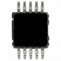
ADC084S021CIMM/NOPB National Semiconductor, ADC084S021CIMM/NOPB Datasheet

ADC084S021CIMM/NOPB
Specifications of ADC084S021CIMM/NOPB
ADC084S021CIMM
ADC084S021CIMMNOPB
ADC084S021CIMMNOPBTR
ADC084S021CIMMNOPBTR
ADC084S021CIMMTR
Available stocks
Related parts for ADC084S021CIMM/NOPB
ADC084S021CIMM/NOPB Summary of contents
Page 1
... ADC124S021 10-bit ADC104S021 8-bit ADC084S021 Connection Diagram TRI-STATE® trademark of National Semiconductor Corporation QSPI™ and SPI™ are trademarks of Motorola, Inc. © 2008 National Semiconductor Corporation Features ■ Specified over a range of sample rates. ■ Four input channels ■ ...
Page 2
Ordering Information Order Code ADC084S021CIMM ADC084S021CIMMX ADC084S021EVAL Block Diagram Pin Descriptions and Equivalent Circuits Pin No. Symbol ANALOG I/O IN1 to IN4 4-7 DIGITAL I/O 10 SCLK 9 DOUT 8 DIN 1 CS POWER SUPPLY GND ...
Page 3
... Absolute Maximum Ratings If Military/Aerospace specified devices are required, please contact the National Semiconductor Sales Office/ Distributors for availability and specifications. Supply Voltage V A Voltage on Any Pin to GND Input Current at Any Pin (Note 3) Package Input Current(Note 3) Power Consumption 25°C A ESD Susceptibility (Note 5) ...
Page 4
Symbol Parameter ANALOG INPUT CHARACTERISTICS V Input Range Leakage Current DCL C Input Capacitance INA DIGITAL INPUT CHARACTERISTICS V Input High Voltage IH V Input Low Voltage IL I Input Current IN C Digital Input Capacitance IND ...
Page 5
ADC084S021 Timing Specifications The following specifications apply for ksps to 200 ksps pF, Boldface limits apply for T SAMPLE L Symbol Parameter t Setup Time SCLK High to CS Falling Edge CSU t ...
Page 6
Timing Diagrams www.national.com ADC084S021 Operational Timing Diagram 20124508 Timing Test Circuit ADC084S021 Serial Timing Diagram 20124550 SCLK and CS Timing Parameters 6 20124551 20124506 ...
Page 7
Specification Definitions ACQUISITION TIME is the time required to acquire the input voltage. That is time required for the hold capacitor to charge up to the input voltage. APERTURE DELAY is the time between the fourth falling SCLK ...
Page 8
Typical Performance Characteristics f = 0.8 MHz to 3.2 MHz 39.9 kHz unless otherwise stated. SCLK IN DNL - V = 3.0V A DNL - V = 5.0V A DNL vs. Supply www.national.com T = +25° ...
Page 9
DNL vs. Clock Frequency 20124524 DNL vs. Clock Duty Cycle 20124526 DNL vs. Temperature 20124528 INL vs. Clock Frequency INL vs. Clock Duty Cycle INL vs. Temperature 9 20124525 20124527 20124529 www.national.com ...
Page 10
SNR vs. Supply SNR vs. Clock Frequency SNR vs. Clock Duty Cycle www.national.com THD vs. Supply 20124530 THD vs. Clock Frequency 20124531 THD vs. Clock Duty Cycle 20124532 10 20124535 20124536 20124537 ...
Page 11
SNR vs. Input Frequency 20124533 SNR vs. Temperature 20124534 SFDR vs. Supply 20124540 THD vs. Input Frequency THD vs. Temperature SINAD vs. Supply 11 20124538 20124539 20124545 www.national.com ...
Page 12
SFDR vs. Clock Frequency SFDR vs. Clock Duty Cycle SFDR vs. Input Frequency www.national.com SINAD vs. Clock Frequency 20124541 SINAD vs. Clock Duty Cycle 20124542 SINAD vs. Input Frequency 20124543 12 20124546 20124547 20124548 ...
Page 13
SFDR vs. Temperature 20124544 ENOB vs. Supply 20124552 ENOB vs. Clock Duty Cycle 20124554 SINAD vs. Temperature ENOB vs. Clock Frequency ENOB vs. Input Frequency 13 20124549 20124553 20124555 www.national.com ...
Page 14
ENOB vs. Temperature Spectral Response - 5V, 200 ksps www.national.com Spectral Response - 3V, 200 ksps 20124556 Power Consumption vs. Throughput 20124560 14 20124559 20124561 ...
Page 15
Applications Information 1.0 ADC084S021 OPERATION The ADC084S021 is a successive-approximation analog-to- digital converter designed around a charge-redistribution dig- ital-to-analog converter. Simplified schematics of the ADC084S021 in both track and hold modes are shown in and , respectively. shows the ADC084S021 ...
Page 16
That is, the conversion that is started at the fall the voltage at the channel that was selected when the last conversion was started. The first conversion after power up will be of the ...
Page 17
ANALOG INPUTS An equivalent circuit for one of the ADC084S021's input chan- nels is shown in Figure 5. Diodes D1 and D2 provide ESD protection for the analog inputs time should any input go beyond (V + ...
Page 18
Physical Dimensions Order Number ADC084S021CIMM, ADC084S021CIMMX www.national.com inches (millimeters) unless otherwise noted 10-Lead MSOP NS Package Number P0MUB10A 18 ...
Page 19
Notes 19 www.national.com ...
Page 20
... For more National Semiconductor product information and proven design tools, visit the following Web sites at: Products Amplifiers www.national.com/amplifiers Audio www.national.com/audio Clock Conditioners www.national.com/timing Data Converters www.national.com/adc Displays www.national.com/displays Ethernet www.national.com/ethernet Interface www.national.com/interface LVDS www.national.com/lvds Power Management www.national.com/power Switching Regulators www.national.com/switchers LDOs www ...


