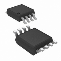
ADC121C021CIMM/NOPB National Semiconductor, ADC121C021CIMM/NOPB Datasheet - Page 14

ADC121C021CIMM/NOPB
Manufacturer Part Number
ADC121C021CIMM/NOPB
Description
IC ADC 12BIT I2C ALERT 8-MSOP
Manufacturer
National Semiconductor
Series
PowerWise®r
Datasheet
1.ADC121C021CIMMNOPB.pdf
(30 pages)
Specifications of ADC121C021CIMM/NOPB
Number Of Bits
12
Sampling Rate (per Second)
188.9k
Data Interface
I²C, Serial
Number Of Converters
1
Power Dissipation (max)
780µW
Voltage Supply Source
Single Supply
Operating Temperature
-40°C ~ 105°C
Mounting Type
Surface Mount
Package / Case
8-TSSOP, 8-MSOP (0.118", 3.00mm Width)
Number Of Elements
1
Resolution
12Bit
Architecture
SAR
Sample Rate
188.9KSPS
Input Polarity
Unipolar
Input Type
Voltage
Rated Input Volt
5.5V
Differential Input
No
Power Supply Requirement
Single
Single Supply Voltage (typ)
3.3/5V
Single Supply Voltage (min)
2.7V
Single Supply Voltage (max)
5.5V
Dual Supply Voltage (typ)
Not RequiredV
Dual Supply Voltage (min)
Not RequiredV
Dual Supply Voltage (max)
Not RequiredV
Differential Linearity Error
-0.9LSB/1LSB
Integral Nonlinearity Error
±1LSB
Operating Temp Range
-40C to 105C
Operating Temperature Classification
Industrial
Mounting
Surface Mount
Pin Count
8
Package Type
MSOP
Input Signal Type
Single-Ended
Lead Free Status / RoHS Status
Lead free / RoHS Compliant
Other names
ADC121C021CIMMTR
www.national.com
1.0 Functional Description
The ADC121C021 is a successive-approximation analog-to-
digital converter designed around a charge-redistribution dig-
ital-to-analog converter. Unless otherwise stated, references
to the ADC121C021 in this section will apply to both the
ADC121C021 and the ADC121C027.
1.1 CONVERTER OPERATION
Simplified schematics of the ADC121C021 in both track and
hold operation are shown in
tively. In
connects the sampling capacitor to the analog input channel,
and SW2 equalizes the comparator inputs. The ADC is in this
state for approximately 0.4µs at the beginning of every con-
version cycle, which begins at the ACK fall of SDA. Conver-
sions occur when the conversion result register is read and
when the ADC is in automatic conversion mode. (see Section
1.9 AUTOMATIC CONVERSION
Figure 3
nects the sampling capacitor to ground and SW2 unbalances
the comparator. The control logic then instructs the charge-
redistribution DAC to add or subtract fixed amounts of charge
to or from the sampling capacitor until the comparator is bal-
anced. At this time the digital word supplied to the DAC is also
the digital representation of the analog input voltage. This
digital word is stored in the conversion result register and read
via the 2-wire interface.
In the Normal (non-Automatic) Conversion mode, a new con-
version is started after the previous conversion result is read.
In the Automatic Mode, conversions are started at set inter-
vals, as determined by bits D7 through D5 of the Configuration
Register. The intent of the Automatic mode is to provide a
"watchdog" function to ensure that the input voltage remains
within the limits set in the Alert Limit Registers. The minimum
and maximum conversion results can then be read from the
Lowest Conversion Register and the Highest Conversion
Register, as described in Section
TERS.
Figure
shows the ADC121C021 in hold mode. SW1 con-
FIGURE 2. ADC121C021 in Track Mode
2, the ADC121C021 is in track mode. SW1
Figure 2
MODE.)
1.6 INTERNAL REGIS-
and
Figure 3
respec-
30020965
14
1.2 ANALOG INPUT
An equivalent circuit for the input of the ADC121C021 is
shown in
analog input. The operating range for the analog input is 0 V
to V
conduct and may result in erratic operation. For this reason,
these diodes should NOT be used to clamp the input signal.
The capacitor C1 in
is mainly the package pin capacitance. Resistor R1 is the on
resistance (R
is typically 500Ω. Capacitor C2 is the ADC121C021 sampling
capacitor, and is typically 30 pF. The ADC121C021 will de-
liver best performance when driven by a low-impedance
source (less than 100Ω). This is especially important when
using the ADC121C021 to sample dynamic signals. A buffer
amplifier may be necessary to limit source impedance. Use a
precision op-amp to maximize circuit performance. Also im-
portant when sampling dynamic signals is a band-pass or low-
pass filter to reduce noise at the input.
The analog input is sampled for eight internal clock cycles, or
for typically 400 ns, after the fall of SDA for acknowledgement.
This time could be as long as about 530 ns. The sampling
switch opens and the conversion begins this time after the fall
of ACK. This time are typical at room temperature and may
vary with temperature.
1.3 ADC TRANSFER FUNCTION
The output format of the ADC121C021 is straight binary.
Code transitions occur midway between successive integer
LSB values. The LSB width for the ADC121C021 is V
The ideal transfer characteristic is shown in
transition from an output code of 0000 0000 0000 to a code
of 0000 0000 0001 is at 1/2 LSB, or a voltage of V
Other code transitions occur at intervals of 1 LSB.
A
. Going beyond this range will cause the ESD diodes to
Figure
FIGURE 3. ADC121C021 in Hold Mode
FIGURE 4. Equivalent Input Circuit
ON
) of the multiplexer and track / hold switch and
4. The diodes provide ESD protection for the
Figure 4
has a typical value of 3 pF and
Figure
30020967
A
A
/ 8192.
/ 4096.
5. The
30020966


