ADC16DV160CILQ/NOPB National Semiconductor, ADC16DV160CILQ/NOPB Datasheet
ADC16DV160CILQ/NOPB
Specifications of ADC16DV160CILQ/NOPB


Related parts for ADC16DV160CILQ/NOPB

ADC16DV160CILQ/NOPB Summary of contents
Page 1
... Dual Supplies: 1.8V and 3.0V operation ■ Selectable input range: 2.4 and 2.0 V ■ Sampling edge flipping with clock divider by 2 option ■ Internal clock divide © 2010 National Semiconductor Corporation ADC16DV160 ■ On-chip low jitter duty-cycle stabilizer ■ Power-down and sleep modes ■ ...
Page 2
Block Diagram www.national.com Functional Block Diagram 2 30101402 ...
Page 3
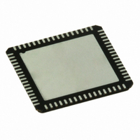
Connection Diagram Ordering Information ≤ Industrial (−40°C +85°C) ADC16DV160CILQ ADC16DV160EB Pin-Out of ADC16DV160 Package 68–pin LLP Evaluation Board 3 30101401 www.national.com ...
Page 4
Pin Descriptions Pin(s) Name ANALOG IN− IN− RPI 10 RPQ RNI 12 RNQ V 2 RMI 16 V RMQ ...
Page 5
Pin(s) Name D1/0+/- D15/14+/- D1/0+/-I to D15/14+/-I 44, 45 OUTCLK+/- POWER SUPPLIES V 4, 14, 22 15, 18, 21, AGND 65 ...
Page 6
... Absolute Maximum Ratings 2) If Military/Aerospace specified devices are required, please contact the National Semiconductor Sales Office/ Distributors for availability and specifications. Supply Voltage (V ) A3.0 Supply Voltage ( A1.8 DR Voltage at any Pin except OUTCLK, CLK CSB, IN SCLK, SDIO, D15/14-D1/0 Voltage at CLK, V Pins IN Voltage at D15/14-D1/0, ...
Page 7
Dynamic Converter Electrical Characteristics Unless otherwise specified, the following specifications apply 160 MSPS at 2 -1dBFS, LVDS R CLK PP IN apply for All other limits apply ...
Page 8
Symbol Parameter +I Output Short Circuit Source Current SC −I Output Short Circuit Source Current SC LVDS Electrical Characteristics Unless otherwise specified, the following specifications apply 160 MSPS at 2 -1dBFS, LVDS R ...
Page 9
Symbol Parameter t CSB Hold Time CSH t Inter-access Gap IAG Note 1: Absolute Maximum Ratings indicate limits beyond which damage to the device may occur. Operating Ratings indicate conditions for which the device is guaranteed to be functional, but ...
Page 10
FIGURE 2. SPI Write Timing FIGURE 3. SPI Read Timing 10 30101412 30101413 ...
Page 11
Specification Definitions APERTURE DELAY is the time after the falling edge of the clock to when the input signal is acquired or held for conver- sion. APERTURE JITTER (APERTURE UNCERTAINTY) is the variation in aperture delay from sample to sample. ...
Page 12
Typical Performance Characteristics, DNL, INL Unless otherwise noted, these specifications apply: V Offset Binary Format. LVDS Rterm = 100 Ω. C DNL DNL vs.V www.national.com = +3.0V A3.0 A1 pF. Typical values are at T ...
Page 13
Typical Performance Characteristics, Dynamic Performance Unless otherwise noted, these specifications apply: V Offset Binary Format. LVDS Rterm = 100 Ω. C SNR, SINAD, SFDR vs. f SNR, SINAD, SFDR vs. V SNR, SINAD, SFDR vs +3.0V ...
Page 14
SNR, SFDR vs. Input Amplitude (dBFS) Spectral Response @ 10.1 MHz Spectral Response at 70 MHz www.national.com SNR, SFDR vs. Input Amplitude (dBc) 30101471 Spectral Response @ 32.5 MHz 30101461 Spectral Response @ 150 MHz 30101463 14 30101472 30101462 30101464 ...
Page 15
Spectral Response @ 197 MHz 30101465 Spectral Response @ 197 MHz, -7dBFS 30101467 Power vs. Temperature 30101427 Spectral Response @ 220 MHz Two Tone Spectral Response @ 197 MHz, 203 MHz 15 30101466 30101468 www.national.com ...
Page 16
Functional Description Operating on dual +1.8V and +3.0V supplies, the AD- C16DV160 digitizes a differential analog input signal to 16 bits, using a differential pipelined architecture with error cor- rection circuitry and an on-chip sample-and-hold circuit to ensure maximum performance. ...
Page 17
Input Common Mode The analog inputs of the ADC16DV160 are not internally dc biased and the range of input common mode is very narrow. Hence it is highly recommended to use the common mode voltage (V , typically 1.15V) as ...
Page 18
The S11 of the input circuit of the ADC16DV160 is shown in Figure 500 MHz predominantly capacitive load- ing with small stray resistance and inductance as shown in Figure 8. An appropriate resistive termination at ...
Page 19
CLOCK INPUT CONSIDERATIONS Clock Input Modes The ADC16DV160 provides a low additive jitter differential clock receiver for optimal dynamic performance over a wide input frequency range. The input common mode of the clock receiver is internally biased at V ...
Page 20
ADC16DV160. Power supplies for the clock drivers have to be separated from the ADC output driver supplies to pre- vent modulating the clock signal with the ADC digital output signals. Higher noise floor and/or increased distortion/spur may result from ...
Page 21
FIGURE 13. Internal References and their Decoupling Reference Decoupling It is highly recommended to place the external decoupling capacitors connected and the pins as possible. The external decoupling capacitors ...
Page 22
For instance, place trans- formers for the analog input and the clock input at 90° to one another to avoid magnetic coupling recommended to place the transformers of the input signal path ...
Page 23
FIGURE 15. Serial Interface Protocol (Read Operation) Signal Descriptions SCLK: Used to register the input date (SDI) on the rising edge; and to source the output data (SDO) on the falling edge. User may disable clock and hold it in ...
Page 24
FIGURE 17. State Machine Generating Fixed Pattern Sequence FIGURE 18. Fixed Pattern at ADC Output with Default SPI Register Values 10.0 SAMPLING EDGE The internal clock divider features allows more flexible design from the perspective of the system clocking scheme. ...
Page 25
Register Map Note: Accessing unspecified addresses may cause functional failure or damage. All reserved bits must be written with the listed default values. Operation Mode Operation Mode Bit 7 Data Format 1 0 Bits (6:5) Operation ...
Page 26
Fixed Pattern Mode: SEQ0 and SEQ1 7 6 SEQ1<2> SEQ1<1> Bits (7:5) 3 bit pattern code for SEQ1. 010 is the default. Bits (4:2) 3 bit pattern code for SEQ0. 010 is the default. Bit 1 Reserved, Must be set ...
Page 27
Fixed Pattern Mode: LSB PATTERN <111> D<7> D<6> D<5> Bits (7:0) 8 LSBs of a fixed pattern for Sequence >111> All '0' for default. Fixed Pattern Mode: MSB PATTERN <1110> D<7> D<6> D<5> Bits (7:0) 8 ...
Page 28
Physical Dimensions www.national.com inches (millimeters) unless otherwise noted 68-Lead LLP Package Ordering Number ADC16DV160CILQ NS Package Number LQA68A 28 ...
Page 29
Notes 29 www.national.com ...
Page 30
... For more National Semiconductor product information and proven design tools, visit the following Web sites at: www.national.com Products Amplifiers www.national.com/amplifiers Audio www.national.com/audio Clock and Timing www.national.com/timing Data Converters www.national.com/adc Interface www.national.com/interface LVDS www.national.com/lvds Power Management www.national.com/power Switching Regulators www.national.com/switchers LDOs www.national.com/ldo LED Lighting www ...