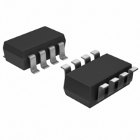
MAX1118EKA+T Maxim Integrated Products, MAX1118EKA+T Datasheet

MAX1118EKA+T
Specifications of MAX1118EKA+T
Related parts for MAX1118EKA+T
MAX1118EKA+T Summary of contents
Page 1
... Systems SPI/QSPI are trademarks of Motorola, Inc. MICROWIRE is a trademark of National Semiconductor, Corp. Functional Diagram appears at end of data sheet. ________________________________________________________________ Maxim Integrated Products For pricing, delivery, and ordering information, please contact Maxim Direct at 1-888-629-4642, or visit Maxim's website at www.maxim-ic.com. Single-Supply, Low-Power, 2-Channel, Serial 8-Bit ADCs ♦ ...
Page 2
Single-Supply, Low-Power, 2-Channel, Serial 8-Bit ADCs ABSOLUTE MAXIMUM RATINGS V to GND ...........................................................-0.3V to +6.0V DD CH0,CH1, REF to GND...............................-0. Digital Output to GND ................................-0. Digital Input to GND ..............................................-0.3V to +6.0V Maximum Current into Any ...
Page 3
ELECTRICAL CHARACTERISTICS (continued +2.7V to +3.6V (MAX1117 unless otherwise noted.) PARAMETER SYMBOL EXTERNAL REFERENCE (MAX1118 ONLY) Input Voltage Range Input Current POWER REQUIREMENTS Supply Voltage Supply Current (Note 2) Supply Rejection Ratio DIGITAL INPUTS (CNVST ...
Page 4
Single-Supply, Low-Power, 2-Channel, Serial 8-Bit ADCs ELECTRICAL CHARACTERISTICS (continued +2.7V to +3.6V (MAX1117 unless otherwise noted.) PARAMETER SYMBOL Serial Clock Falling Edge to DOUT Serial Clock Rising Edge to DOUT High-Z Last Serial Clock to ...
Page 5
V = +5V (MAX1119 +25°C, unless otherwise noted.) A MAX1117/MAX1119 SUPPLY CURRENT vs. CONVERSION RATE 100.0 MAX1119 10 +5V DD 1.0 MAX1117 V = +3V DD 0.1 0.01 0.1 ...
Page 6
Single-Supply, Low-Power, 2-Channel, Serial 8-Bit ADCs (V = +3V (MAX1117 +5V (MAX1119 +25°C, unless otherwise noted.) A MAX1118 OFFSET ERROR vs. SUPPLY VOLTAGE 0 2.048V REF 0.4 0.3 0.2 0.1 0 ...
Page 7
V = +5V (MAX1119 +25°C, unless otherwise noted.) A REFERENCE VOLTAGE vs. NUMBER OF PIECES 21.0% 17.5% 14.0% 10.5% 7.0% 3.5% 0 3.980 4.020 4.060 REFERENCE VOLTAGE (V) PIN NAME 1 ...
Page 8
Single-Supply, Low-Power, 2-Channel, Serial 8-Bit ADCs DOUT DOUT 3kΩ C LOAD GND HIGH Figure 1. Load Circuits for Enable Time V CH0 DD 0.1μF ANALOG INPUTS GND CH1 MAX1117 MAX1118 MAX1119 ...
Page 9
Since the device requires only a single supply, the negative input of the comparator is set to equal V /2. The capacitive DAC DD restores the positive input within the limits of ...
Page 10
... SCLK cause serial data to be output. Falling edges on CNVST, during an active conversion process, interrupt the current conver- sion and cause the input multiplexer to switch to CH1. To reinitiate a conversion on CH0 necessary to AutoShutdown is a trademark of Maxim Integrated Products. 10 ______________________________________________________________________________________ POWER-DOWN MODE t ...
Page 11
ACTIVE t csh CH0 CH1 CNVST t conv IDLE LOW SCLK t csd D OUT Figure 6c. Conversion and Interface Timing, Conversion on CH1 with SCLK Idle Low ACTIVE t csh CH0 CH1 CNVST t conv SCLK IDLE HIGH t ...
Page 12
Single-Supply, Low-Power, 2-Channel, Serial 8-Bit ADCs OUTPUT CODE FULL-SCALE TRANSITION 11111111 11111110 11111101 00000011 00000010 00000001 00000000 INPUT VOLTAGE (LSB) Figure 7. Input/Output Transfer Function Applications Information Power-On Reset When power is first applied, the MAX1117/MAX1118/ ...
Page 13
SCLK CNVST CH0 INPUT MULTIPLEXER CH1 should be low impedance and as short as possible for noise-free operation. High-frequency noise in the V DD affect the comparator in the ADC. Bypass the supply to the star ground with a 0.1µF ...
Page 14
... Maxim cannot assume responsibility for use of any circuitry other than circuitry entirely embodied in a Maxim product. No circuit patent licenses are implied. Maxim reserves the right to change the circuitry and specifications without notice at any time. 14 ____________________Maxim Integrated Products, 120 San Gabriel Drive, Sunnyvale, CA 94086 408-737-7600 © 2000 Maxim Integrated Products Printed USA is a registered trademark of Maxim Integrated Products ...


