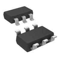
ADC121C021CIMK/NOPB National Semiconductor, ADC121C021CIMK/NOPB Datasheet - Page 27

ADC121C021CIMK/NOPB
Manufacturer Part Number
ADC121C021CIMK/NOPB
Description
IC ADC 12BIT I2C ALERT TSOT23-6
Manufacturer
National Semiconductor
Series
PowerWise®r
Datasheet
1.ADC121C021CIMMNOPB.pdf
(30 pages)
Specifications of ADC121C021CIMK/NOPB
Number Of Bits
12
Sampling Rate (per Second)
188.9k
Data Interface
I²C, Serial
Number Of Converters
1
Power Dissipation (max)
780µW
Voltage Supply Source
Single Supply
Operating Temperature
-40°C ~ 105°C
Mounting Type
Surface Mount
Package / Case
SOT-23-6 Thin, TSOT-23-6
Lead Free Status / RoHS Status
Lead free / RoHS Compliant
Other names
ADC121C021CIMK
ADC121C021CIMK
ADC121C021CIMKTR
ADC121C021CIMK
ADC121C021CIMKTR
2.0 Applications Information
2.1 TYPICAL APPLICATION CIRCUIT
A typical application circuit is shown in
supply is bypassed with a capacitor network located close to
the ADC121C021. The ADC uses the analog supply (V
its reference voltage, so it is very important that V
clean as possible. Due to the low power requirements of the
ADC121C021, it is possible to use a precision reference as a
power supply.
The bus pull-up resistors (R
controller's supply. It is important that the pull-up resistors are
pulled to the same voltage potential as V
that the logic levels of all devices on the bus are compatible.
2.2 BUFFERED INPUT
A buffered input application circuit is shown in
analog input is buffered by a National Semiconductor
LMP7731. The non-inverting amplifier configuration provides
a buffered gain stage for a single ended source. This appli-
cation circuit is good for single-ended sensor interface. The
P
) should be powered by the
Figure
A
. This will ensure
FIGURE 18. Typical Application Circuit
18. The analog
Figure
FIGURE 19. Buffered Input Circuit
A
be kept as
19. The
A
) as
27
If the controller's supply is noisy, an appropriate bypass ca-
pacitor should be added between the controller's supply pin
and the pull-up resistors. For Hs-mode applications, this by-
pass capacitance will improve the accuracy of the ADC.
The value of the pull-up resistors (R
characteristics of each particular I
tion describes how to choose an appropriate value. As a
general rule-of-thumb, we suggest using a 1kΩ resistor for
Hs-mode bus configurations and a 5kΩ resistor for Standard
or Fast Mode bus configurations. Depending upon the bus
capacitance, these values may or may not be sufficient to
meet the timing requirements of the I
Please see the I
input must have a DC bias level that keeps the ADC input
signal from swinging below GND or above the supply (+5V in
this case).
The LM4132, with its 0.05% accuracy over temperature, is an
excellent choice as a reference source for the ADC121C021.
2
C specification for further information.
30020921
2
C bus. The I
P
30020920
2
) depends upon the
C bus specification.
2
www.national.com
C specifica-


