MAX118CAI+ Maxim Integrated Products, MAX118CAI+ Datasheet
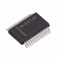
IC ADC 8BIT 1MSPS 28-SSOP

MAX118CAI+

Manufacturer Part Number
MAX118CAI+
Description
IC ADC 8BIT 1MSPS 28-SSOP
Manufacturer
Maxim Integrated Products
Datasheet

Specifications of MAX118CAI+

Number Of Bits
8
Sampling Rate (per Second)
1M
Data Interface
Parallel
Number Of Converters
3
Power Dissipation (max)
762mW
Voltage Supply Source
Single Supply
Operating Temperature
0°C ~ 70°C
Mounting Type
Surface Mount
Package / Case
28-SSOP
Number Of Adc Inputs
8
Architecture
Semiflash
Conversion Rate
1000 KSPs
Resolution
8 bit
Input Type
Voltage
Voltage Reference
External
Supply Voltage (max)
5 V
Maximum Power Dissipation
762 mW
Maximum Operating Temperature
+ 70 C
Mounting Style
SMD/SMT
Minimum Operating Temperature
0 C
Lead Free Status / RoHS Status
Lead free / RoHS Compliant
The MAX114/MAX118 are microprocessor-compatible,
8-bit, 4-channel and 8-channel analog-to-digital con-
verters (ADCs). They operate from a single +5V supply
and use a half-flash technique to achieve a 660ns con-
version time (1Msps). A power-down (PWRDN) pin
reduces current consumption typically to 1µA. The
devices return from power-down mode to normal oper-
ating mode in less than 200ns, allowing large supply-
current reductions in burst-mode applications (in burst
mode, the ADC wakes up from a low-power state at
specified intervals to sample the analog input signals).
Both converters include a track/hold, enabling the ADC
to digitize fast analog signals.
Microprocessor (µP) interfaces are simplified because the
ADC can appear as a memory location or I/O port without
external interface logic. The data outputs use latched,
three-state buffer circuitry for direct connection to an 8-bit
parallel µP data bus or system input port. The
MAX114/MAX118 input/reference configuration enables
ratiometric operation.
The 4-channel MAX114 is available in a 24-pin DIP or
SSOP. The 8-channel MAX118 is available in a 28-pin
DIP or SSOP. For +3V applications, refer to the
MAX113/MAX117 data sheet.
________________________Applications
19-1083; Rev 1; 8/96
For free samples & the latest literature: http://www.maxim-ic.com, or phone 1-800-998-8800
_________________________________________________________Functional Diagram
_______________General Description
High-Speed DSP
Portable Equipment
* MAX118 ONLY
________________________________________________________________ Maxim Integrated Products
*IN7
*IN6
*IN5
IN4
IN3
IN2
IN1
Remote Data Acquisition
Communications Systems
*IN8
A0
ADDRESS
DECODE
MUX
LATCH
A1
8-Bit ADCs with 1µA Power-Down
A2
+5V, 1Msps, 4 & 8-Channel,
REF-
PWRDN
REF+
16
REF+
____________________________Features
Ordering Information continued on last page.
*Dice are specified at T
**Contact factory for availability.
Pin Configurations appear on last page.
MODE
______________Ordering Information
MAX114CNG
MAX114CAG
MAX114C/D
MAX114ENG
MAX114EAG
MAX114MRG
Single +5V Supply Operation
4 (MAX114) or 8 (MAX118) Analog Input Channels
Low Power: 40mW (operating mode)
Total Unadjusted Error ≤1LSB
Fast Conversion Time: 660ns per Channel
No External Clock Required
Internal Track/Hold
1MHz Full-Power Bandwidth
Internally Connected 8th Channel Monitors
Reference Voltage (MAX118)
TIMING AND
4-BIT
DAC
CONTROL
(4LSBs)
FLASH
4-BIT
RD
ADC
PART
(4MSBs)
FLASH
4-BIT
ADC
INT
CS
WR/RDY
5µW (power-down mode)
MAX114/MAX118
TEMP. RANGE
-40°C to +85°C
-40°C to +85°C
-55°C to +125°C
0°C to +70°C
0°C to +70°C
0°C to +70°C
A
= +25°C, DC parameters only.
DRIVERS
OUTPUT
THREE-
STATE
D7
D6
D5
D4
D3
D2
D1
D0
24 Narrow Plastic DIP
24 SSOP
Dice*
24 Narrow Plastic DIP
24 SSOP
24 Narrow CERDIP**
PIN-PACKAGE
1

Related parts for MAX118CAI+

MAX118CAI+ Summary of contents

Page 1

... IN1 ADDRESS LATCH DECODE MAX118 ONLY ________________________________________________________________ Maxim Integrated Products For free samples & the latest literature: http://www.maxim-ic.com, or phone 1-800-998-8800 +5V, 1Msps, 4 & 8-Channel, ____________________________Features Single +5V Supply Operation 4 (MAX114 (MAX118) Analog Input Channels Low Power: 40mW (operating mode) Total Unadjusted Error ≤1LSB ...

Page 2

ADCs with 1µA Power-Down ABSOLUTE MAXIMUM RATINGS V to GND ..............................................................-0.3V to +7V DD Digital Input Voltage to GND ......................-0. Digital Output Voltage to GND ...................-0. REF+ to GND..............................................-0.3V to ...

Page 3

ADCs with 1µA Power-Down ELECTRICAL CHARACTERISTICS (continued +5V ±5%, REF+ = 5V, REF- = GND, Read Mode (MODE = GND PARAMETER SYMBOL LOGIC INPUTS Input High Voltage V INH Input Low Voltage V INL Input ...

Page 4

ADCs with 1µA Power-Down TIMING CHARACTERISTICS (V = +4.75V +25°C, unless otherwise noted.) (Note PARAMETER SYMBOL CONDITIONS Conversion Time t < INTL t CWR (Note 5) (WR-RD ...

Page 5

ADCs with 1µA Power-Down __________________________________________Typical Operating Characteristics (V = +5V +25°C, unless otherwise noted CONVERSION TIME vs. AMBIENT TEMPERATURE 1.5 1.4 1.3 1 +4.75V 1.1 DD 1.0 0.9 0 +5V 0.7 ...

Page 6

ADCs with 1µA Power-Down ______________________________________________________________Pin Description PIN NAME MAX114 MAX118 — 1 IN6 — 2 IN5 1 3 IN4 2 4 IN3 3 5 IN2 4 6 IN1 5 7 MODE ...

Page 7

ADCs with 1µA Power-Down _______________Detailed Description Converter Operation The MAX114/MAX118 use a half-flash conversion tech- nique (see Functional Diagram ) in which two 4-bit flash ADC sections achieve an 8-bit result. Using 15 com- parators, the flash ADC compares ...

Page 8

ADCs with 1µA Power-Down In read mode, WR/RDY is configured as a status output (RDY can drive the ready or wait input of a µP. RDY is an open-collector output (no internal ...

Page 9

ADCs with 1µA Power-Down Pipelined Operation Besides the two standard write-read-mode options, pipelined operation can be achieved by connecting (Figure 6). With CS low, driving WR and RD low initiates a conversion and concurrently reads the ...

Page 10

ADCs with 1µA Power-Down to break this current path during power-down. The FET should have an on-resistance of less than 2Ω with a 5V gate drive. When REF- is switched Figure 7d, ...

Page 11

ADCs with 1µA Power-Down Transfer Function Figure 10 shows the MAX114/MAX118’s nominal trans- fer function. Code transitions occur halfway between successive-integer LSB values. Output coding is binary with 1LSB = ( 256. REF+ REF- Conversion ...

Page 12

... Maxim reserves the right to change the circuitry and specifications without notice at any time. implied. Maxim reserves the right to change the circuitry and specifications without notice at any time. 12 __________________Maxim Integrated Products, 120 San Gabriel Drive, Sunnyvale, CA 94086 (408) 737-7600 12 __________________Maxim Integrated Products, 120 San Gabriel Drive, Sunnyvale, CA 94086 (408) 737-7600 © ...

Related keywords